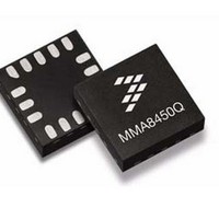
MMA8450QT Freescale Semiconductor, MMA8450QT Datasheet - Page 43

MMA8450QT
Manufacturer Part Number
MMA8450QT
Description
Board Mount Accelerometers 12bit 3-Axis FIFO HPF PL
Manufacturer
Freescale Semiconductor
Specifications of MMA8450QT
Sensing Axis
X, Y, Z
Acceleration
2 g, 4 g, 8 g
Digital Output - Number Of Bits
12 bit
Supply Voltage (max)
1.89 V
Supply Voltage (min)
1.71 V
Supply Current
3 uA
Maximum Operating Temperature
+ 85 C
Minimum Operating Temperature
- 40 C
Shutdown
Yes
Sensitivity
0.976 mg/digit, 1.953 mg/digit, 3.906 mg/digit
Package / Case
QFN-16
Output Type
Digital
Package Type
QFN
Operating Temperature (min)
-40C
Operating Temperature (max)
85C
Operating Temperature Classification
Industrial
Product Depth (mm)
3mm
Product Height (mm)
1mm
Product Length (mm)
3mm
Mounting
Surface Mount
Pin Count
16
Acceleration Range
± 2g, ± 4g, ± 8g
No. Of Axes
3
Ic Interface Type
I2C, Serial
Sensor Case Style
QFN
No. Of Pins
16
Supply Voltage Range
1.71V To 1.89V
Rohs Compliant
Yes
Lead Free Status / RoHS Status
Lead free / RoHS Compliant
Available stocks
Company
Part Number
Manufacturer
Quantity
Price
Company:
Part Number:
MMA8450QT
Manufacturer:
RALINK
Quantity:
2 940
Part Number:
MMA8450QT
Manufacturer:
FREESCALE
Quantity:
20 000
Table 61. OFF_X Description
Table 62. OFF_Y Description
system’s interrupt controller. The interrupt controller routes the enabled functional block interrupt to the INT1 or INT2 pin.
0x3C: CTRL_REG5 Interrupt Configuration Register
the routing table for the INT1 and INT2 interrupt pins. If the bit value is logic ‘0’ the functional block’s interrupt is routed to INT2,
and if the bit value is logic ‘1’ then the interrupt is routed to INT1. One or more functions can assert an interrupt pin; therefore a
host application responding to an interrupt should read the INT_SOURCE (0x15) register to determine the appropriate sources
of the interrupt.
6.8
complement offset correction registers values are used to realign the Zero-g position of the X, Y, and Z-axis after device board
mount. The resolution of the offset registers is 3.906 mg per LSB. The 2’s complement 8-bit value would result in an offset
compensation range ±0.5g.
0x3D: OFF_X Offset Correction X Register
0x3E: OFF_Y Offset Correction Y Register
0x3F: OFF_Z Offset Correction Z Register
0x3C CTRL_REG5 Register (Read/Write)
0x3D OFF_X Register (Read/Write)
0x3E OFF_Y Register (Read/Write)
Table 63. OFF_Z Description
Sensors
Freescale Semiconductor
Table 60. Interrupt Configuration Register Description
0x3F OFF_Z Register (Read/Write)
INT_CFG_ASLP
The corresponding functional block interrupt enable bit allows the functional block to route its event detection flags to the
The system’s interrupt controller shown in
For more information on how to calibrate the 0g Offset refer to AN3916 Offset Calibration Using the MMA8450Q. The 2’s
D7-D0
D7-D0
D7-D0
Bit 7
Bit 7
Interrupt Configuration
Bit 7
Bit 7
D7
D7
D7
INT_CFG_FF_MT_1
INT_CFG_FF_MT_2
INT_CFG_LNDPRT
INT_CFG_TRANS
INT_CFG_PULSE
INT_CFG_DRDY
INT_CFG_ASLP
INT_CFG_FIFO
User Offset Correction Registers
Y-axis offset trim LSB value. Default value: 0000_0000.
X -axis offset trim LSB value. Default value: 0000_0000.
Z-axis offset trim LSB value. Default value: 0000_0000.
INT_CFG_FIFO
Bit 6
Bit 6
Bit 6
Bit 6
D6
D6
D6
INT_CFG_TRANS INT_CFG_LNDPRT INT_CFG_PULSE INT_CFG_FF_MT_1INT_CFG_FF_MT_2 INT_CFG_DRDY
INT1/INT2 Configuration. Default value: 0.
0: Interrupt is routed to INT2 pin; 1: Interrupt is routed to INT1 pin
INT1/INT2 Configuration. Default value: 0.
0: Interrupt is routed to INT2 pin; 1: Interrupt is routed to INT1 pin
INT1/INT2 Configuration. Default value: 0.
0: Interrupt is routed to INT2 pin; 1: Interrupt is routed to INT1 pin
INT1/INT2 Configuration. Default value: 0.
0: Interrupt is routed to INT2 pin; 1: Interrupt is routed to INT1 pin
INT1/INT2 Configuration. Default value: 0.
0: Interrupt is routed to INT2 pin; 1: Interrupt is routed to INT1 pin
INT1/INT2 Configuration. Default value: 0.
0: Interrupt is routed to INT2 pin; 1: Interrupt is routed to INT1 pin
INT1/INT2 Configuration. Default value: 0.
0: Interrupt is routed to INT2 pin; 1: Interrupt is routed to INT1 pin
INT1/INT2 Configuration. Default value: 0.
0: Interrupt is routed to INT2 pin; 1: Interrupt is routed to INT1 pin
Bit 5
Bit 5
Bit 5
Bit 5
D5
D5
D5
Figure 10
Bit 4
Bit 4
Bit 4
Bit 4
D4
D4
D4
uses the corresponding bit field in the CTRL_REG5 register to determine
Bit 3
Bit 3
Bit 3
Bit 3
D3
D3
D3
Description
Bit 2
Bit 2
Bit 2
Bit 2
D2
D2
D2
Bit 1
Bit 1
Bit 1
Bit 1
D1
D1
D1
MMA8450Q
Bit 0
Bit 0
Bit 0
Bit 0
D0
D0
D0
43


