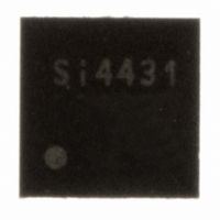
SI4431-A0-FM Silicon Laboratories Inc, SI4431-A0-FM Datasheet - Page 58

SI4431-A0-FM
Manufacturer Part Number
SI4431-A0-FM
Description
IC TXRX ISM 930MHZ 3.6V 20-QFN
Manufacturer
Silicon Laboratories Inc
Specifications of SI4431-A0-FM
Package / Case
20-QFN
Mfg Application Notes
Transitioning SI4430/31 to Rev B
Frequency
240MHz ~ 930MHz
Data Rate - Maximum
128kbps
Modulation Or Protocol
FSK, GFSK, OOK
Power - Output
13dBm
Sensitivity
-118dBm
Voltage - Supply
1.8 V ~ 3.6 V
Current - Receiving
18.5mA
Current - Transmitting
28mA
Data Interface
PCB, Surface Mount
Antenna Connector
PCB, Surface Mount
Operating Temperature
-40°C ~ 85°C
Number Of Receivers
2
Number Of Transmitters
1
Wireless Frequency
240 MHz to 930 MHz
Output Power
13 dBm
Operating Supply Voltage
1.8 V to 3.6 V
Maximum Operating Temperature
+ 85 C
Mounting Style
SMD/SMT
Maximum Supply Current
28 mA
Minimum Operating Temperature
- 40 C
Modulation
FSK, GFSK, OOK
Lead Free Status / RoHS Status
Lead free / RoHS Compliant
Applications
-
Memory Size
-
Lead Free Status / RoHS Status
Lead free / RoHS Compliant, Lead free / RoHS Compliant
Other names
336-1633-5
Available stocks
Company
Part Number
Manufacturer
Quantity
Price
Company:
Part Number:
SI4431-A0-FMR
Manufacturer:
SILICON
Quantity:
3 500
Part Number:
SI4431-A0-FMR
Manufacturer:
SILICONLABS/芯科
Quantity:
20 000
Si4431
8.3.1. ADC Differential Input Mode—Bridge Sensor Example
The differential input mode of ADC8 is designed to directly interface any bridge-type sensor, which is demonstrated
in the figure below. As seen in the figure the use of the ADC in this configuration will utilize two GPIO pins. The
supply source of the bridge and chip should be the same to eliminate the measuring error caused by battery
discharging. For proper operation one of the VDD dependent references (VDD/2 or VDD/3) should be selected for
the reference voltage of ADC8. VDD/2 reference should be selected for VDD lower than 2.7 V, VDD/3 reference
should be selected for VDD higher than 2.7 V. The differential input mode supports programmable gain to match
the input range of ADC8 to the characteristic of the sensor and VDD proportional programmable offset adjustment
to compensate the offset of the sensor.
The adcgain[1:0] bits in "Register 0Eh. I/O Port Configuration" determine the gain of the differential/single ended
amplifier. This is used to fit the input range of the ADC8 to bridge sensors having different sensitivity:
Note: The input range is the differential voltage measured between the selected GPIO pins corresponding to the full ADC
58
adcgain[1]
range (255).
The gain is different for different VDD dependent references so the reference change has no influence on input range
and digital measured values.
0
0
1
1
adcgain[0]
Figure 25. ADC Differential Input Example—Bridge Sensor
Microcontroller
Digital I/O
GND
0
1
0
1
adcref[0] = 0
measure control
+
22/13
44/13
66/13
88/13
Differential Gain
Preliminary Rev. 0.4
+
adcref[0] = 1
132/13
33/13
66/13
99/13
-
VDD
GPIO2
GPIO1
GND
Tamara
Input Range (% of VDD)
16.7
8.4
5.6
4.2


