SI4431-A0-FM Silicon Laboratories Inc, SI4431-A0-FM Datasheet - Page 155
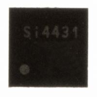
SI4431-A0-FM
Manufacturer Part Number
SI4431-A0-FM
Description
IC TXRX ISM 930MHZ 3.6V 20-QFN
Manufacturer
Silicon Laboratories Inc
Specifications of SI4431-A0-FM
Package / Case
20-QFN
Mfg Application Notes
Transitioning SI4430/31 to Rev B
Frequency
240MHz ~ 930MHz
Data Rate - Maximum
128kbps
Modulation Or Protocol
FSK, GFSK, OOK
Power - Output
13dBm
Sensitivity
-118dBm
Voltage - Supply
1.8 V ~ 3.6 V
Current - Receiving
18.5mA
Current - Transmitting
28mA
Data Interface
PCB, Surface Mount
Antenna Connector
PCB, Surface Mount
Operating Temperature
-40°C ~ 85°C
Number Of Receivers
2
Number Of Transmitters
1
Wireless Frequency
240 MHz to 930 MHz
Output Power
13 dBm
Operating Supply Voltage
1.8 V to 3.6 V
Maximum Operating Temperature
+ 85 C
Mounting Style
SMD/SMT
Maximum Supply Current
28 mA
Minimum Operating Temperature
- 40 C
Modulation
FSK, GFSK, OOK
Lead Free Status / RoHS Status
Lead free / RoHS Compliant
Applications
-
Memory Size
-
Lead Free Status / RoHS Status
Lead free / RoHS Compliant, Lead free / RoHS Compliant
Other names
336-1633-5
Available stocks
Company
Part Number
Manufacturer
Quantity
Price
Company:

Part Number:
SI4431-A0-FMR
Manufacturer:
SILICON
Quantity:
3 500
Part Number:
SI4431-A0-FMR
Manufacturer:
SILICONLABS/芯科
Quantity:
20 000


13. Pin Descriptions: Si4431
PKG
Pin
10
12
13
20
21
22
23
24
25
26
11
1
2
3
4
5
6
7
8
9
PADDLE_GND
Pin Name
VDD_DIG
VDD_RF
GPIO_0
GPIO_1
GPIO_2
VR_IF
XOUT
SCLK
nSEL
nIRQ
SDO
VDR
SDN
RXp
RXn
SDI
XIN
NC
NC
TX
GND
VDD
VDD
I/O
I/O
I/O
I/O
—
—
O
O
O
O
O
O
I
I
I
I
I
I
I
+1.8 to +3.6 V supply voltage input to all analog +1.7 V regulators. The recommended V
is +3.3 V.
Transmit output pin. The maximum level in TX mode is +13 dBm. The PA output is an open-drain connec-
tion so the L-C match must supply VDD (+3.3 VDC nominal) to this pin.
Differential RF input pins of the LNA. See application schematic for example matching network.
Regulated Output Voltage of the IF 1.7 V Regulator. A 1 µF decoupling capacitor is required.
No Connect.
General Purpose Digital I/O that may be configured through the registers to perform various functions
including: Microcontroller Clock Output, FIFO status, POR, Wake-Up timer, Low Battery Detect, TRSW,
AntDiversity control, etc. See the SPI GPIO Configuration Registers, Address 0Bh, 0Ch, and 0Dh for
more information.
Regulated Output Voltage of the Digital 1.7 V Regulator. A 1 µF decoupling capacito is required.
No Connect.
+1.8 to +3.6 V supply voltage input to the Digital +1.7 V Regulator. The recommended V
is +3.3 V.
0–V
Serial Data input. 0–V
bus.
Serial Clock input. 0–V
serial data bus. Data is clocked into the Si4431 on positive edge transitions.
Serial Interface Select input. 0– V
line serial data bus. The signal is also used to signify burst read/write mode.
General Microcontroller Interrupt Status output. When the Si4431 exhibits anyone of the Interrupt Events
the nIRQ pin will be set low=0. Please see the Control Logic registers section for more information on the
Interrupt Events. The Microcontroller can then determine the state of the interrupt by reading a corre-
sponding SPI Interrupt Status Registers, Address 03h and 04h.
Crystal Oscillator Output. Connect to an external 30 MHz crystal or leave floating if driving the Xin pin with
an external signal source.
Crystal Oscillator Input. Connect to an external 30 MHz crystal or to an external source. If using an exter-
nal clock source with no crystal, dc coupling with a nominal 0.8 VDC level is recommended with a mini-
mum ac amplitude of 700 mVpp.
Shutdown input pin. 0–V
SDN =1 the chip will be completely shutdown and the contents of the registers will be lost.
The exposed metal paddle on the bottom of the Si4431 supplies the RF and circuit ground(s) for the entire
chip. It is very important that a good solder connection is made between this exposed metal paddle and
the ground plane of the PCB underlying the Si4431.
DD
V digital output that provides a serial readback function of the internal control registers.
VDD_RF
VR_IF
Paddle
RXp
RXn
Metal
TX
DD
Preliminary Rev. 0.4
DD
DD
1
2
3
4
5
V digital input. This pin provides the serial data stream for the 4-line serial data
V digital input. This pin provides the serial data clock function for the 4-line
V digital input. SDN should be = 0 in all modes except Shutdown mode. When
20
6
19 18 17
7
8
DD
9
V digital input. This pin provides the Select/Enable function for the 4-
10
16
15
14
13
12
11
Description
SCLK
SDI
SDO
VDD_DIG
NC
Si4431
DD
DD
supply voltage
supply voltage
155
Related parts for SI4431-A0-FM
Image
Part Number
Description
Manufacturer
Datasheet
Request
R

Part Number:
Description:
IC TXRX 240-930MHZ -8-13DB 20QFN
Manufacturer:
Silicon Laboratories Inc
Datasheet:

Part Number:
Description:
IC TXRX 240-930MHZ -8-13DB 20QFN
Manufacturer:
Silicon Laboratories Inc
Datasheet:
Part Number:
Description:
SMD/C°/SINGLE-ENDED OUTPUT SILICON OSCILLATOR
Manufacturer:
Silicon Laboratories Inc
Part Number:
Description:
Manufacturer:
Silicon Laboratories Inc
Datasheet:
Part Number:
Description:
N/A N/A/SI4010 AES KEYFOB DEMO WITH LCD RX
Manufacturer:
Silicon Laboratories Inc
Datasheet:
Part Number:
Description:
N/A N/A/SI4010 SIMPLIFIED KEY FOB DEMO WITH LED RX
Manufacturer:
Silicon Laboratories Inc
Datasheet:
Part Number:
Description:
N/A/-40 TO 85 OC/EZLINK MODULE; F930/4432 HIGH BAND (REV E/B1)
Manufacturer:
Silicon Laboratories Inc
Part Number:
Description:
EZLink Module; F930/4432 Low Band (rev e/B1)
Manufacturer:
Silicon Laboratories Inc
Part Number:
Description:
I°/4460 10 DBM RADIO TEST CARD 434 MHZ
Manufacturer:
Silicon Laboratories Inc
Part Number:
Description:
I°/4461 14 DBM RADIO TEST CARD 868 MHZ
Manufacturer:
Silicon Laboratories Inc
Part Number:
Description:
I°/4463 20 DBM RFSWITCH RADIO TEST CARD 460 MHZ
Manufacturer:
Silicon Laboratories Inc
Part Number:
Description:
I°/4463 20 DBM RADIO TEST CARD 868 MHZ
Manufacturer:
Silicon Laboratories Inc
Part Number:
Description:
I°/4463 27 DBM RADIO TEST CARD 868 MHZ
Manufacturer:
Silicon Laboratories Inc
Part Number:
Description:
I°/4463 SKYWORKS 30 DBM RADIO TEST CARD 915 MHZ
Manufacturer:
Silicon Laboratories Inc