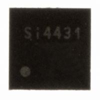
SI4431-A0-FM Silicon Laboratories Inc, SI4431-A0-FM Datasheet - Page 19

SI4431-A0-FM
Manufacturer Part Number
SI4431-A0-FM
Description
IC TXRX ISM 930MHZ 3.6V 20-QFN
Manufacturer
Silicon Laboratories Inc
Specifications of SI4431-A0-FM
Package / Case
20-QFN
Mfg Application Notes
Transitioning SI4430/31 to Rev B
Frequency
240MHz ~ 930MHz
Data Rate - Maximum
128kbps
Modulation Or Protocol
FSK, GFSK, OOK
Power - Output
13dBm
Sensitivity
-118dBm
Voltage - Supply
1.8 V ~ 3.6 V
Current - Receiving
18.5mA
Current - Transmitting
28mA
Data Interface
PCB, Surface Mount
Antenna Connector
PCB, Surface Mount
Operating Temperature
-40°C ~ 85°C
Number Of Receivers
2
Number Of Transmitters
1
Wireless Frequency
240 MHz to 930 MHz
Output Power
13 dBm
Operating Supply Voltage
1.8 V to 3.6 V
Maximum Operating Temperature
+ 85 C
Mounting Style
SMD/SMT
Maximum Supply Current
28 mA
Minimum Operating Temperature
- 40 C
Modulation
FSK, GFSK, OOK
Lead Free Status / RoHS Status
Lead free / RoHS Compliant
Applications
-
Memory Size
-
Lead Free Status / RoHS Status
Lead free / RoHS Compliant, Lead free / RoHS Compliant
Other names
336-1633-5
Available stocks
Company
Part Number
Manufacturer
Quantity
Price
Company:
Part Number:
SI4431-A0-FMR
Manufacturer:
SILICON
Quantity:
3 500
Part Number:
SI4431-A0-FMR
Manufacturer:
SILICONLABS/芯科
Quantity:
20 000
3. Controller Interface
3.1. Serial Peripheral Interface (SPI)
The Si4431 communicates with the host MCU over a 3 wire SPI interface: SCLK, SDI, and nSEL. The host MCU
can also read data from internal registers on the SDO output pin. A SPI transaction is a 16-bit sequence which
consists of a Read-Write (R/W) select bit, followed by a 7-bit address field (ADDR), and an 8-bit data field (DATA),
as demonstrated in Figure 2. The 7-bit address field supports reading from or writing to one of the 128, 8-bit control
registers. The R/W select bit determines whether the SPI transaction is a write or read transaction. If R/W = 1, it
signifies a WRITE transaction, while R/W = 0 signifies a READ transaction. The contents (ADDR or DATA) are
latched into the Si4431 every eight clock cycles. The timing parameters for the SPI interface are shown in Table 10.
The SCLK rate is flexible with a maximum rate of 10 MHz.
To read back data from the Si4431, the R/W bit must be set to 0 followed by the 7-bit address of the register from
which to read. The 8 bit DATA field following the 7-bit ADDR field is ignored when R/W = 0. The next eight negative
edge transitions of the SCLK signal will clock out the contents of the selected register. The data read from the
selected register will be available on the SDO output pin. The READ function is shown in Figure 3. After the READ
function is completed the SDO pin will remain at either a logic 1 or logic 0 state depending on the last data bit
clocked out (D0). When nSEL goes high the SDO output pin will be pulled high by internal pullup.
Symbol
t
t
t
t
t
t
t
t
t
t
SW
CH
DS
DH
DD
EN
DE
SH
CL
SS
SCLK
nSEL
Output data delay time
Output disable time
Output enable time
Select high period
Select setup time
SDI
Select hold time
Data setup time
Clock high time
Clock low time
Data hold time
Parameter
MSB
RW
A6 A5
Table 10. Serial Interface Timing Parameters
Min (nsec)
A4
Address
50
80
40
40
20
20
20
20
50
20
A3
Figure 2. SPI Timing
A2 A1 A0 D7 D6 D5 D4 D3 D2 D1 D0
Preliminary Rev. 0.4
SDI
SCLK
SDO
nSEL
t
t
EN
SS
Data
t
CL
t
CH
Diagram
t
DS
t
DH
LSB
t
DD
xx xx
t
SH
Si4431
RW A7
t
DE
t
SW
19


