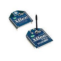
XBP09-DPSIT-156 Digi International, XBP09-DPSIT-156 Datasheet - Page 8

XBP09-DPSIT-156
Manufacturer Part Number
XBP09-DPSIT-156
Description
MODULE XBEE PRO W/RPSMA
Manufacturer
Digi International
Series
XBEE-PRO™r
Specifications of XBP09-DPSIT-156
Frequency
902MHz ~ 928MHz
Data Rate - Maximum
156kbps
Modulation Or Protocol
FHSS
Applications
ISM
Power - Output
17dBm (50mW)
Sensitivity
-100dBm
Voltage - Supply
3 V ~ 3.6 V
Current - Receiving
80mA
Current - Transmitting
210mA
Data Interface
PCB, Through Hole
Antenna Connector
RP-SMA
Operating Temperature
-40°C ~ 85°C
Package / Case
Module
Lead Free Status / RoHS Status
Lead free / RoHS Compliant
Memory Size
-
Lead Free Status / Rohs Status
Lead free / RoHS Compliant
Other names
602-1169
XBee‐PRO® 900 RF Modules
Pin #
18
19
20
Design Notes
AD0 / DIO0 / Commissioning
AD2 / DIO2
AD1 / DIO1
Name
Button
Power Supply Design
Recommended Pin Connections
Board Layout
Pin Assignments for the XBee‐PRO® 900 Modules
The XBee modules do not specifically require any external circuitry or specific connections for
proper operation. However, there are some general design guidelines that are recommended for
help in troubleshooting and building a robust design.
Poor power supply can lead to poor radio performance especially if the supply voltage is not kept
within tolerance or is excessively noisy. To help reduce noise a 1.0 uF and 8.2pF capacitor are
recommended to be placed as near to pin1 on the PCB as possible. If using a switching regulator
for your power supply, switching frequencies above 500kHz are preferred. Power supply ripple
should be limited to a maximum 100mV peak to peak. To ensure proper power up, Vcc SLOPE
must be superior or equal to 6V/ms.
The only required pin connections are VCC, GND, DOUT and DIN. To support serial firmware
updates, VCC, GND, DOUT, DIN, RTS, and DTR should be connected.
All unused pins should be left disconnected. All inputs on the radio can be pulled high with internal
pull-up resistors using the PR software command. No specific treatment is needed for unused
outputs.
Other pins may be connected to external circuitry for convenience of operation including the
Associate LED pin (pin 15) and the commissioning button pin (pin 20). The Associate LED pin will
flash differently depending on the state of the module, and a pushbutton attached to pin 20 can
enable various deployment and troubleshooting functions without having to send UART
commands.
The combined source and sink capabilities of the module are limited to 120mA for all pins on the
module. Module pins 11 and 15 can source/sink a maximum of 2mA; pins 9, 6, and 13 can source/
sink a maximum of 16mA; and all other pins can source/sink a maximum of 8mA.
If analog sampling is desired the VRef pin (pin 14) should be attached to a voltage reference.
XBee modules do not have any specific sensitivity to nearby processors, crystals or other PCB
components. Other than mechanical considerations, no special PCB placement is required for
integrating XBee radios. In general, Power and GND traces should be thicker than signal traces
and be able to comfortably support the maximum currents.
The radios are also designed to be self sufficient and work with the integrated and external
antennas without the need for additional ground planes on the host PCB. Large ground planes on a
host PCB should not adversely affect maximum range, but they may affect radiation patterns of
onboard XBee antennas.
© 2009 Digi International, Inc.
(Low‐asserted signals are distinguished with a horizontal line above signal name.)
Direction
Either
Either
Either
Analog Input 0, Digital I/O 0, or Commissioning Button
Analog Input 2 or Digital I/O 2
Analog Input 1 or Digital I/O 1
Description
Max Voltage
Vcc
Vcc
Vcc
8


