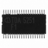
TDA5251 Infineon Technologies, TDA5251 Datasheet - Page 51

TDA5251
Manufacturer Part Number
TDA5251
Description
TXRX FSK/ASK SGL LP TSSOP-38
Manufacturer
Infineon Technologies
Type
Transceiverr
Specifications of TDA5251
Package / Case
38-TSSOP
Frequency
315MHz
Data Rate - Maximum
64kbps
Modulation Or Protocol
ASK, FSK
Applications
RKE, Remote Control Systems
Power - Output
13dBm
Sensitivity
-109dBm
Voltage - Supply
2.1 V ~ 5.5 V
Current - Receiving
9.3mA
Current - Transmitting
14mA
Data Interface
PCB, Surface Mount
Antenna Connector
PCB, Surface Mount
Operating Temperature
-40°C ~ 85°C
Operating Frequency
0.35 MHz
Operating Supply Voltage
2.5 V, 3.3 V, 5 V
Maximum Operating Temperature
+ 85 C
Minimum Operating Temperature
- 40 C
Mounting Style
SMD/SMT
Operating Temperature (min)
-40C
Operating Temperature (max)
85C
Operating Temperature Classification
Industrial
Product Depth (mm)
4.4mm
Product Length (mm)
9.7mm
Operating Supply Voltage (min)
2.1V
Operating Supply Voltage (max)
5.5V
Lead Free Status / RoHS Status
Lead free / RoHS Compliant
Memory Size
-
Lead Free Status / Rohs Status
Compliant
Other names
SP000014554
TDA5251
TDA5251INTR
TDA5251XT
TDA5251
TDA5251INTR
TDA5251XT
Available stocks
Company
Part Number
Manufacturer
Quantity
Price
Company:
Part Number:
TDA5251
Manufacturer:
INFINEON
Quantity:
276
e.g.
with a frequency deviation of 30kHz.
Figure 3-15 shows the configuration of the switches and the capacitors to achieve the 2 desired
frequencies. Gray parts of the schematics indicate inactive parts. For FSK modulation the ASK-
switch is always open.
For FSK LOW the FSK-switch is closed and C
by:
For finetuning C tune1 can be varied over a range of 8 pF in steps of 125fF. The switches of this C-
bank are controlled by the bits D0 to D5 in the FSK register (subaddress 01H, see Table 3-6).
For FSK HIGH the FSK-switch is open. So the effective C
The C-bank C tune2 can be varied over a range of 16 pF in steps of 250fF for finetuning of the FSK
HIGH frequency. The switches of this C-bank are controlled by the bits D8 to D13 in the FSK
register (subaddress 01H, see Table 3-6).
Figure 3-15
Data Sheet
C
C
C
C v+
V
V1
V2
−
f
f
COSC HI
COSC LOW
=
=
C
f, C
C
(
-------------------------------------------------------------------------------------- -
V3
C
C v1
v
L
1
v1
FSK modulation
XSWA 22
XOUT 19
XSWF 20
XGND 23
+
+
XIN 21
+
C
C
C tune1
tune1
tune
= (315E6 + 30E3) / 24= 13.12625MHz
= (315E6 - 30E3) / 24= 13.12375MHz
FSK LOW
1
)
+
⋅
L
(
C v2
C
v2
+
+
C tune2
C
C
C
-R
tune2
tune1
tune2
)
v2
51
and C
C
C
V1
V2
tune2
C
f, C
v+
V3
are bypassed. The effective C
L
is given by:
XSWA 22
XOUT 19
XSWF 20
XGND 23
XIN 21
FSK HIGH
[3 – 20]
[3 – 21]
L
C
C
-R
tune2
tune1
TDA5251 F1
Version 1.1
Application
2007-02-26
QOSC_FSK.wmf
v-
is given


