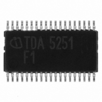
TDA5251 Infineon Technologies, TDA5251 Datasheet - Page 23

TDA5251
Manufacturer Part Number
TDA5251
Description
TXRX FSK/ASK SGL LP TSSOP-38
Manufacturer
Infineon Technologies
Type
Transceiverr
Specifications of TDA5251
Package / Case
38-TSSOP
Frequency
315MHz
Data Rate - Maximum
64kbps
Modulation Or Protocol
ASK, FSK
Applications
RKE, Remote Control Systems
Power - Output
13dBm
Sensitivity
-109dBm
Voltage - Supply
2.1 V ~ 5.5 V
Current - Receiving
9.3mA
Current - Transmitting
14mA
Data Interface
PCB, Surface Mount
Antenna Connector
PCB, Surface Mount
Operating Temperature
-40°C ~ 85°C
Operating Frequency
0.35 MHz
Operating Supply Voltage
2.5 V, 3.3 V, 5 V
Maximum Operating Temperature
+ 85 C
Minimum Operating Temperature
- 40 C
Mounting Style
SMD/SMT
Operating Temperature (min)
-40C
Operating Temperature (max)
85C
Operating Temperature Classification
Industrial
Product Depth (mm)
4.4mm
Product Length (mm)
9.7mm
Operating Supply Voltage (min)
2.1V
Operating Supply Voltage (max)
5.5V
Lead Free Status / RoHS Status
Lead free / RoHS Compliant
Memory Size
-
Lead Free Status / Rohs Status
Compliant
Other names
SP000014554
TDA5251
TDA5251INTR
TDA5251XT
TDA5251
TDA5251INTR
TDA5251XT
Available stocks
Company
Part Number
Manufacturer
Quantity
Price
Company:
Part Number:
TDA5251
Manufacturer:
INFINEON
Quantity:
276
Table 2-6
The I
parameters at any time.
It is possible to set the device in three different modes: Slave Mode, Self Polling Mode and Timer
Mode. This is done by a state machine which is implemented in the WAKEUP LOGIC unit. A
detailed description is given in Section 2.4.16.
The DATA VALID DETECTOR contains a frequency window counter and an RSSI threshold
comparator. The window counter uses the incoming data signal from the data slicer as the gating
signal and the crystal oscillator frequency as the timebase to determine the actual datarate. The
result is compared with the expected datarate.
The threshold comparator compares the actual RSSI level with the expected RSSI level.
If both conditions are true the PwdDD pin is set to LOW in self polling mode as you can see in
Section 2.4.16. This signal can be used as an interrupt for an external µP. Because the PwdDD
pin is bidirectional and open drain driven by an internal pull-up resistor it is possible to apply an
external LOW thus enabling the device.
2.4.15
The TDA5251 supports the I
selectable by the BusMode pin (pin 2) as shown in the following table. All bus pins (BusData,
BusCLK, EN, BusMode) have a Schmitt-triggered input stage. The BusData pin is bidirectional
where the output is open drain driven by an internal 15kΩ pull up resistor.
Figure 2-7
Note: The Interface is able to access the internal registers at any time, even in POWER DOWN
mode. There is no internal clock necessary for Interface operation.
Data Sheet
3-wire Mode
2
Function
I
2
C / 3-wire Bus Interface gives an external microcontroller full control over important system
C Mode
Bus Interface and Register Definition
Bus Interface Format
Bus Interface
BusMode
High
Low
BusMode
BusData
BusCLK
2
C bus protocol (2 wire) and a 3-wire bus protocol. Operation is
EN
16
17
24
2
High= inactive,
Low= active
EN
23
1 1 1 0 0 0 0 0
INTERFACE
CHIP ADDRESS
I
2
C / 3-wire
INTERNAL BUS
Clock input
BusCLK
Functional Description
Data in/out
TDA5251 F1
BusData
Version 1.1
2007-02-26
i2c_3w_bus.wmf


