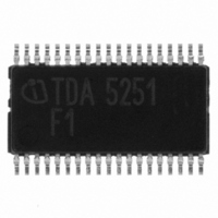
TDA5251 Infineon Technologies, TDA5251 Datasheet - Page 27

TDA5251
Manufacturer Part Number
TDA5251
Description
TXRX FSK/ASK SGL LP TSSOP-38
Manufacturer
Infineon Technologies
Type
Transceiverr
Specifications of TDA5251
Package / Case
38-TSSOP
Frequency
315MHz
Data Rate - Maximum
64kbps
Modulation Or Protocol
ASK, FSK
Applications
RKE, Remote Control Systems
Power - Output
13dBm
Sensitivity
-109dBm
Voltage - Supply
2.1 V ~ 5.5 V
Current - Receiving
9.3mA
Current - Transmitting
14mA
Data Interface
PCB, Surface Mount
Antenna Connector
PCB, Surface Mount
Operating Temperature
-40°C ~ 85°C
Operating Frequency
0.35 MHz
Operating Supply Voltage
2.5 V, 3.3 V, 5 V
Maximum Operating Temperature
+ 85 C
Minimum Operating Temperature
- 40 C
Mounting Style
SMD/SMT
Operating Temperature (min)
-40C
Operating Temperature (max)
85C
Operating Temperature Classification
Industrial
Product Depth (mm)
4.4mm
Product Length (mm)
9.7mm
Operating Supply Voltage (min)
2.1V
Operating Supply Voltage (max)
5.5V
Lead Free Status / RoHS Status
Lead free / RoHS Compliant
Memory Size
-
Lead Free Status / Rohs Status
Compliant
Other names
SP000014554
TDA5251
TDA5251INTR
TDA5251XT
TDA5251
TDA5251INTR
TDA5251XT
Available stocks
Company
Part Number
Manufacturer
Quantity
Price
Company:
Part Number:
TDA5251
Manufacturer:
INFINEON
Quantity:
276
Subaddress Organization
Table 2-13
Table 2-14
Data Byte Specification
Table 2-15
Note D3: Function is only active in selfpolling and timer mode. When D3 is set to LOW the RX path
is not enabled if PwdDD pin is set to LOW. A delayed setting of D3 results in a delayed power ON
of the RX building blocks.
Data Sheet
MSB
MSB
1
1
0
0
0
0
0
0
0
0
0
0
0
0
D15
D14
D13
D12
D11
D10
Bit
D9
D8
D7
D6
D5
D4
D3
D2
D1
D0
0
0
0
0
0
0
0
0
0
0
0
0
0
0
0
0
0
0
0
0
0
0
0
0
0
0
0
0
F_COUNT_MODE
0
0
RX_DATA_INV
0
0
0
0
0
0
0
0
0
0
0
0
Sub Addresses of Data Registers Write
Sub Addresses of Data Registers Read
Sub Address 00H: CONFIG
TESTMODE
ADC_MODE
ASK_NFSK
CONTROL
LNA_GAIN
Function
PA_PWR
MODE_2
MODE_1
RX_NTX
CLK_EN
ALL_PD
SLICER
D_OUT
EN_RX
0
0
0
0
0
0
0
0
0
0
1
1
1
1
0
0
0
0
0
0
1
1
1
1
0
1
1
1
0
0
0
0
1
1
0
0
1
1
0
0
1
1
LSB HEX
0
1
LSB
0
1
0
1
0
1
0
1
0
1
0
1
0= disable receiver, 1= enable receiver (in self polling and timer mode) *
80h
81h
0= RX/TX and ASK/FSK external controlled, 1= Register controlled
HEX
0= CLK off during power down, 1= always CLK on, ever in PD
0Dh
0Eh
00h
01h
02h
03h
04h
05h
06h
07h
08h
0Fh
Function
STATUS
XTAL_TUNING
XTAL_CONFIG
COUNT_TH1
COUNT_TH2
0= slave or timer mode, 1= self polling mode
ADC
BLOCK_PD
OFF_TIME
RSSI_TH3
ON_TIME
Function
CLK_DIV
CONFIG
0= normal operation, 1= all Power down
0= no Data inversion, 1= Data inversion
0= Data out if valid, 1= always Data out
0= low TX Power, 1= high TX Power
FSK
LPF
0= normal operation, 1=Testmode
0= Lowpass, 1= Peak Detector
0= slave mode, 1= timer mode
27
0= one shot, 1= continuous
0= one shot, 1= continuous
0= low gain, 1= high gain
0= FSK, 1=ASK
Results of comparison: ADC & WINDOW
0= TX, 1=RX
Description
Configuration and Ratio of clock divider
I/Q and data filter cutoff frequencies
Higher threshold of window counter
Lower threshold of window counter
General definition of status bits
Building Blocks Power Down
OFF time of wakeup counter
ON time of wakeup counter
Threshold for RSSI signal
Values for FSK-shift
XTAL configuration
Nominal frequency
ADC data out
Description
Description
Functional Description
TDA5251 F1
Version 1.1
2007-02-26
Bit Length
Bit Length
Default
0
0
0
0
0
1
0
0
1
1
1
1
1
0
0
1
8
8
16
16
16
16
16
16
16
16
8
8
8
8


