MRF24J40-I/ML Microchip Technology, MRF24J40-I/ML Datasheet - Page 9
MRF24J40-I/ML
Manufacturer Part Number
MRF24J40-I/ML
Description
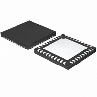
IC TXRX IEEE/ZIGBEE 2.4GHZ 40QFN
Manufacturer
Microchip Technology
Specifications of MRF24J40-I/ML
Package / Case
40-QFN
Frequency
2.4GHz
Data Rate - Maximum
250kbps
Modulation Or Protocol
802.15.4
Applications
ISM, ZigBee™
Power - Output
0dBm
Sensitivity
-95dBm
Voltage - Supply
2.4 V ~ 3.6 V
Current - Receiving
18mA
Current - Transmitting
18mA
Data Interface
PCB, Surface Mount
Antenna Connector
PCB, Surface Mount
Operating Temperature
-40°C ~ 85°C
Number Of Receivers
1
Number Of Transmitters
1
Wireless Frequency
2.4 GHz
Interface Type
4 Wire SPI
Noise Figure
8 dB
Output Power
+ 0 dBm
Operating Supply Voltage
2.5 V, 3.3 V
Maximum Operating Temperature
85 C
Mounting Style
SMD/SMT
Maximum Supply Current
22 mA
Minimum Operating Temperature
- 40 C
Lead Free Status / RoHS Status
Lead free / RoHS Compliant
Memory Size
-
Lead Free Status / Rohs Status
Lead free / RoHS Compliant
Available stocks
Company
Part Number
Manufacturer
Quantity
Price
Company:

Part Number:
MRF24J40-I/ML
Manufacturer:
MICROCHIP
Quantity:
12 000
Part Number:
MRF24J40-I/ML
Manufacturer:
MICROCHIP/微芯
Quantity:
20 000


2.3
TABLE 2-1:
© 2010 Microchip Technology Inc.
Legend: A = Analog, D = Digital, I = Input, O = Output
Pin
12
13
10
11
14
15
16
17
18
19
20
21
22
23
24
25
26
27
28
29
30
31
32
33
34
35
36
37
38
39
40
1
2
3
4
5
6
7
8
9
Pin Descriptions
LPOSC2
LPOSC1
Symbol
RESET
GPIO0
GPIO1
GPIO5
GPIO4
GPIO2
GPIO3
WAKE
OSC2
OSC1
LCAP
GND
GND
SDO
GND
GND
GND
GND
RFN
SCK
RFP
V
V
V
V
V
V
V
V
V
INT
SDI
CS
NC
NC
NC
NC
NC
DD
DD
DD
DD
DD
DD
DD
DD
DD
MRF24J40 PIN DESCRIPTIONS
Ground
Ground
Ground
Ground
Ground
Ground
Power
Power
Power
Power
Power
Power
Power
Power
Power
Type
AIO
AIO
DIO
DIO
DIO
DIO
DIO
DIO
DO
DO
DI
DI
DI
DI
DI
—
—
—
—
—
—
AI
AI
AI
AI
RF power supply. Bypass with a capacitor as close to the pin as possible.
Differential RF input/output (+).
Differential RF input/output (-).
RF power supply. Bypass with a capacitor as close to the pin as possible.
Guard ring power supply. Bypass with a capacitor as close to the pin as possible.
Guard ring ground.
General purpose digital I/O, also used as external PA enable.
General purpose digital I/O, also used as external TX/RX switch control.
General purpose digital I/O.
General purpose digital I/O.
General purpose digital I/O, also used as external TX/RX switch control.
General purpose digital I/O.
Global hardware Reset pin active-low.
Ground for digital circuit.
External wake-up trigger (must be enabled in software).
Interrupt pin to microcontroller.
Serial interface data output from MRF24J40.
Serial interface data input to MRF24J40.
Serial interface clock.
Serial interface enable.
Digital circuit power supply. Bypass with a capacitor as close to the pin as possible.
Ground for digital circuit.
No Connection.
Ground for digital circuit.
Ground for digital circuit.
No Connection. (Allow pin to float; do not connect signal.)
32 kHz crystal input.
32 kHz crystal input.
No Connection. (Allow pin to float; do not connect signal.)
No Connection. (Allow pin to float; do not connect signal.)
Power supply for band gap reference circuit. Bypass with a capacitor as close to the
pin as possible.
Power supply for analog circuit. Bypass with a capacitor as close to the pin as
possible.
20 MHz crystal input.
20 MHz crystal input.
PLL power supply. Bypass with a capacitor as close to the pin as possible.
Ground for PLL.
Charge pump power supply. Bypass with a capacitor as close to the pin as possible.
No Connection.
VCO supply. Bypass with a capacitor as close to the pin as possible.
PLL loop filter external capacitor. Connected to external 100 pF capacitor.
Preliminary
Description
MRF24J40
DS39776C-page 9
Related parts for MRF24J40-I/ML
Image
Part Number
Description
Manufacturer
Datasheet
Request
R

Part Number:
Description:
IEEE 802.15.4� 2.4 GHz RF Transceiver
Manufacturer:
MICROCHIP [Microchip Technology]
Datasheet:

Part Number:
Description:
Ieee 802.15.4? 2.4 Ghz Rf Transceiver
Manufacturer:
Microchip Technology Inc.
Datasheet:
Part Number:
Description:
Manufacturer:
Microchip Technology Inc.
Datasheet:
Part Number:
Description:
Manufacturer:
Microchip Technology Inc.
Datasheet:
Part Number:
Description:
Manufacturer:
Microchip Technology Inc.
Datasheet:
Part Number:
Description:
Manufacturer:
Microchip Technology Inc.
Datasheet:
Part Number:
Description:
Manufacturer:
Microchip Technology Inc.
Datasheet:
Part Number:
Description:
Manufacturer:
Microchip Technology Inc.
Datasheet:
Part Number:
Description:
Manufacturer:
Microchip Technology Inc.
Datasheet:
Part Number:
Description:
Manufacturer:
Microchip Technology Inc.
Datasheet: