MRF24J40-I/ML Microchip Technology, MRF24J40-I/ML Datasheet - Page 151
MRF24J40-I/ML
Manufacturer Part Number
MRF24J40-I/ML
Description
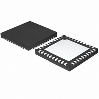
IC TXRX IEEE/ZIGBEE 2.4GHZ 40QFN
Manufacturer
Microchip Technology
Specifications of MRF24J40-I/ML
Package / Case
40-QFN
Frequency
2.4GHz
Data Rate - Maximum
250kbps
Modulation Or Protocol
802.15.4
Applications
ISM, ZigBee™
Power - Output
0dBm
Sensitivity
-95dBm
Voltage - Supply
2.4 V ~ 3.6 V
Current - Receiving
18mA
Current - Transmitting
18mA
Data Interface
PCB, Surface Mount
Antenna Connector
PCB, Surface Mount
Operating Temperature
-40°C ~ 85°C
Number Of Receivers
1
Number Of Transmitters
1
Wireless Frequency
2.4 GHz
Interface Type
4 Wire SPI
Noise Figure
8 dB
Output Power
+ 0 dBm
Operating Supply Voltage
2.5 V, 3.3 V
Maximum Operating Temperature
85 C
Mounting Style
SMD/SMT
Maximum Supply Current
22 mA
Minimum Operating Temperature
- 40 C
Lead Free Status / RoHS Status
Lead free / RoHS Compliant
Memory Size
-
Lead Free Status / Rohs Status
Lead free / RoHS Compliant
Available stocks
Company
Part Number
Manufacturer
Quantity
Price
Company:

Part Number:
MRF24J40-I/ML
Manufacturer:
MICROCHIP
Quantity:
12 000
Part Number:
MRF24J40-I/ML
Manufacturer:
MICROCHIP/微芯
Quantity:
20 000


Reset .................................................................................. 85
Revision History ............................................................... 141
RF Transceiver ................................................................ 129
RSSI
RSSI/ED
© 2010 Microchip Technology Inc.
SLPCAL2 (Sleep Calibration 2) ................................. 64
SLPCON0 (Sleep Clock Control 0) ............................ 66
SLPCON1 (Sleep Clock Control 1) ............................ 66
SOFTRST (Software Reset) ...................................... 44
SYMTICKH (Symbol Period Tick High Byte) ............. 29
SYMTICKL (Symbol Period Tick Low Byte) ............... 29
TESTMODE (Test Mode) ........................................... 71
TRISGPIO (GPIO Pin Direction) ................................ 51
TXBCON0 (Transmit Beacon FIFO Control 0) ........... 32
TXBCON1 (Transmit Beacon Control 1) .................... 40
TXG1CON (GTS1 FIFO Control) ............................... 34
TXG2CON (GTS2 FIFO Control) ............................... 34
TXMCR (CSMA-CA Mode Control) ............................ 26
TXNCON (Transmit Normal FIFO Control) ................ 33
TXPEND (TX Data Pending) ...................................... 36
TXSTAT (TX MAC Status) ......................................... 39
TXSTBL (TX Stabilization) ......................................... 47
TXTIME (TX Turnaround Time) ................................. 42
UPNONCE0 (Upper Nonce Security 0) ..................... 77
UPNONCE1 (Upper Nonce Security 1) ..................... 77
UPNONCE10 (Upper Nonce Security 10) ................. 82
UPNONCE11 (Upper Nonce Security 11) ................. 82
UPNONCE12 (Upper Nonce Security 12) ................. 83
UPNONCE2 (Upper Nonce Security 2) ..................... 78
UPNONCE3 (Upper Nonce Security 3) ..................... 78
UPNONCE4 (Upper Nonce Security 4) ..................... 79
UPNONCE5 (Upper Nonce Security 5) ..................... 79
UPNONCE6 (Upper Nonce Security 6) ..................... 80
UPNONCE7 (Upper Nonce Security 7) ..................... 80
UPNONCE8 (Upper Nonce Security 8) ..................... 81
UPNONCE9 (Upper Nonce Security 9) ..................... 81
WAKECON (Wake Control) ....................................... 37
WAKETIMEH (Wake-up Time Match
WAKETIMEL (Wake-up Time Match
Associated Registers ................................................. 85
Mode 1 ....................................................................... 90
Mode 2 ....................................................................... 90
Associated Registers ................................................. 90
Value High) ........................................................ 67
Value Low) ......................................................... 67
Preliminary
S
Schematic ........................................................................ 133
Security ............................................................................ 123
Security
Setting Up Beacon-Enabled/Nonbeacon-Enabled Networks
Short Address Control Register Summary ......................... 15
Sleep ............................................................................... 115
Sleep Timer
T
Timing Diagrams
Transmission ................................................................... 106
Turbo Mode ..................................................................... 128
TX Beacon FIFO .............................................................. 109
TX FIFOs Frame Structure .............................................. 108
TX GTSx FIFO ................................................................. 110
TX Normal FIFO .............................................................. 108
W
WWW Address ................................................................ 146
WWW, On-Line Support ...................................................... 2
MAC Sublayer Receive Decryption ......................... 125
MAC Sublayer Transmit Encryption ........................ 123
Memory Map ............................................................ 123
Upper Layer Decryption ........................................... 127
Upper Layer Encryption ........................................... 126
Associated Registers ............................................... 127
Associated Registers ................................................. 98
Associated Registers ............................................... 121
Beacon-Enabled Coordinator Mode ........................ 118
Beacon-Enabled Device Mode ................................ 119
Immediate Sleep and Wake-up Mode ..................... 121
Nonbeacon-Enabled (Coordinator or
Timed Sleep Mode .................................................. 115
Example SPI Slave Mode ........................................ 137
External PA/LNA ...................................................... 131
Long Address Read ................................................... 13
Long Address Write ................................................... 13
Short Address Read .................................................. 12
Short Address Write .................................................. 12
SPI Port Read (Output) ............................................. 10
SPI Port Write (Input) ................................................ 10
Associated Registers ............................................... 111
Associated Registers ............................................... 128
Device) Mode .................................................. 120
MRF24J40
DS39776C-page 151
Related parts for MRF24J40-I/ML
Image
Part Number
Description
Manufacturer
Datasheet
Request
R

Part Number:
Description:
IEEE 802.15.4� 2.4 GHz RF Transceiver
Manufacturer:
MICROCHIP [Microchip Technology]
Datasheet:

Part Number:
Description:
Ieee 802.15.4? 2.4 Ghz Rf Transceiver
Manufacturer:
Microchip Technology Inc.
Datasheet:
Part Number:
Description:
Manufacturer:
Microchip Technology Inc.
Datasheet:
Part Number:
Description:
Manufacturer:
Microchip Technology Inc.
Datasheet:
Part Number:
Description:
Manufacturer:
Microchip Technology Inc.
Datasheet:
Part Number:
Description:
Manufacturer:
Microchip Technology Inc.
Datasheet:
Part Number:
Description:
Manufacturer:
Microchip Technology Inc.
Datasheet:
Part Number:
Description:
Manufacturer:
Microchip Technology Inc.
Datasheet:
Part Number:
Description:
Manufacturer:
Microchip Technology Inc.
Datasheet:
Part Number:
Description:
Manufacturer:
Microchip Technology Inc.
Datasheet: