MRF24J40-I/ML Microchip Technology, MRF24J40-I/ML Datasheet - Page 150
MRF24J40-I/ML
Manufacturer Part Number
MRF24J40-I/ML
Description
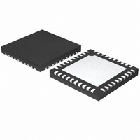
IC TXRX IEEE/ZIGBEE 2.4GHZ 40QFN
Manufacturer
Microchip Technology
Specifications of MRF24J40-I/ML
Package / Case
40-QFN
Frequency
2.4GHz
Data Rate - Maximum
250kbps
Modulation Or Protocol
802.15.4
Applications
ISM, ZigBee™
Power - Output
0dBm
Sensitivity
-95dBm
Voltage - Supply
2.4 V ~ 3.6 V
Current - Receiving
18mA
Current - Transmitting
18mA
Data Interface
PCB, Surface Mount
Antenna Connector
PCB, Surface Mount
Operating Temperature
-40°C ~ 85°C
Number Of Receivers
1
Number Of Transmitters
1
Wireless Frequency
2.4 GHz
Interface Type
4 Wire SPI
Noise Figure
8 dB
Output Power
+ 0 dBm
Operating Supply Voltage
2.5 V, 3.3 V
Maximum Operating Temperature
85 C
Mounting Style
SMD/SMT
Maximum Supply Current
22 mA
Minimum Operating Temperature
- 40 C
Lead Free Status / RoHS Status
Lead free / RoHS Compliant
Memory Size
-
Lead Free Status / Rohs Status
Lead free / RoHS Compliant
Available stocks
Company
Part Number
Manufacturer
Quantity
Price
Company:

Part Number:
MRF24J40-I/ML
Manufacturer:
MICROCHIP
Quantity:
12 000
Part Number:
MRF24J40-I/ML
Manufacturer:
MICROCHIP/微芯
Quantity:
20 000


MRF24J40
Pins
Power and Ground Pins ....................................................... 8
Power Management
Proprietary Protocols
Proprietary Wireless Networking Protocols .......................... 1
R
Reader Response ............................................................ 147
Received Signal Strength Indicator (RSSI) ........................ 90
Reception ......................................................................... 103
Recommended Operating Conditions .............................. 136
Registers
DS39776C-page 150
OSC1 (20 MHz Crystal Input) ...................................... 7
OSC2 (20 MHz Crystal Input) ...................................... 7
RESET (Global Hardware Reset Active-Low) .............. 7
RFN (Differential RF Pin, Negative) ............................. 7
RFP (Differential RF Pin, Positive) ............................... 7
SCK (Serial Interface Clock) ........................................ 7
SDI (Serial Interface Data Input) .................................. 7
SDO (Serial Interface Data Output) ............................. 7
V
V
V
V
V
V
V
V
WAKE (External Wake-up Trigger) .............................. 7
General Purpose Input/Output (GPIO) ......................... 9
Interrupt (INT) .............................................................. 9
Reset (RESET) ............................................................ 9
Serial Peripheral Interface (SPI) ................................ 10
Wake (WAKE) .............................................................. 9
Associated Registers ............................................... 114
MiWi ............................................................................. 1
MiWi P2P ..................................................................... 1
ZigBee .......................................................................... 1
Acknowledgement Request ..................................... 104
Associated Registers ............................................... 105
Interrupt .................................................................... 104
Modes ...................................................................... 104
ACKTMOUT (MAC ACK Time-out Duration) ............. 27
ASSOEADR0 (Associated Coordinator
ASSOEADR1 (Associated Coordinator
ASSOEADR2 (Associated Coordinator
ASSOEADR3 (Associated Coordinator
ASSOEADR4 (Associated Coordinator
ASSOEADR5 (Associated Coordinator
ASSOEADR6 (Associated Coordinator
ASSOEADR7 (Associated Coordinator
ASSOSADR0 (Associated Coordinator
DD
DD
DD
DD
DD
DD
DD
DD
(Charge Pump Power Supply) .............................. 7
(Digital Circuit Power Supply) ............................... 7
(Guard Ring Power Supply) .................................. 7
(PLL Power Supply) .............................................. 7
(Power Supply, Analog Circuit) ............................. 7
(Power Supply, Band Gap
(RF Power Supply) ............................................... 7
(VCO Supply) ....................................................... 7
Reference Circuit) ................................................ 7
Error ................................................................. 104
Normal ............................................................. 104
Promiscuous .................................................... 104
Extended Address 0) ......................................... 72
Extended Address 1) ......................................... 72
Extended Address 2) ......................................... 73
Extended Address 3) ......................................... 73
Extended Address 4) ......................................... 74
Extended Address 5) ......................................... 74
Extended Address 6) ......................................... 75
Extended Address 7) ......................................... 75
Short Address 0) ................................................ 76
Preliminary
ASSOSADR1 (Associated Coordinator
BBREG0 (Baseband 0) .............................................. 55
BBREG1 (Baseband 1) .............................................. 55
BBREG2 (Baseband 2) .............................................. 56
BBREG3 (Baseband 3) .............................................. 56
BBREG4 (Baseband 4) .............................................. 57
BBREG6 (Baseband 6) .............................................. 57
CCAEDTH (Energy Detection
EADR0 (Extended Address 0) ................................... 21
EADR1 (Extended Address 1) ................................... 21
EADR2 (Extended Address 2) ................................... 21
EADR3 (Extended Address 3) ................................... 22
EADR4 (Extended Address 4) ................................... 22
EADR5 (Extended Address 5) ................................... 22
EADR6 (Extended Address 6) ................................... 23
EADR7 (Extended Address 7) ................................... 23
ESLOTG1 (GTS1 and CAP End Slot) ....................... 28
ESLOTG23 (End Slot of GTS3 and GTS2) ............... 35
ESLOTG45 (End Slot of GTS5 and GTS4) ............... 35
ESLOTG67 (End Slot of GTS6) ................................. 35
FRMOFFSET (Superframe Counter Offset
GATECLK (Gated Clock Control) .............................. 41
GPIO (GPIO Port) ...................................................... 51
HSYMTMRH (Half Symbol Timer High Byte) ............ 43
HSYMTMRL (Half Symbol Timer Low Byte) .............. 43
INTCON (Interrupt Control) ........................................ 50
INTSTAT (Interrupt Status) ........................................ 49
MAINCNT0 (Main Counter 0) .................................... 69
MAINCNT1 (Main Counter 1) .................................... 69
MAINCNT2 (Main Counter 2) .................................... 70
MAINCNT3 (Main Counter 3) .................................... 70
ORDER (Beacon and Superframe Order) ................. 25
PACON0 (Power Amplifier Control 0) ........................ 30
PACON1 (Power Amplifier Control 1) ........................ 30
PACON2 (Power Amplifier Control 2) ........................ 31
PANIDH (PAN ID High Byte) ..................................... 19
PANIDL (PAN ID Low Byte) ....................................... 19
REMCNTH (Remain Counter High) ........................... 68
REMCNTL (Remain Counter Low) ............................ 68
RFCON0 (RF Control 0) ............................................ 59
RFCON1 (RF Control 1) ............................................ 59
RFCON2 (RF Control 2) ............................................ 60
RFCON3 (RF Control 3) ............................................ 60
RFCON5 (RF Control 5) ............................................ 61
RFCON6 (RF Control 6) ............................................ 61
RFCON7 (RF Control 7) ............................................ 62
RFCON8 (RF Control 8) ............................................ 62
RFCTL (RF Mode Control) ........................................ 53
RFSTATE (RF State) ................................................. 65
RSSI (Averaged RSSI Value) .................................... 65
RXFLUSH (Receive FIFO Flush) ............................... 24
RXMCR (Receive MAC Control) ................................ 18
RXSR (RX MAC Status) ............................................ 48
SADRH (Short Address High Byte) ........................... 20
SADRL (Short Address Low Byte) ............................. 20
SECCON0 (Security Control 0) ................................. 45
SECCON1 (Security Control 1) ................................. 46
SECCR2 (Security Control 2) .................................... 54
SLPACK (Sleep Acknowledgement and
SLPCAL0 (Sleep Calibration 0) ................................. 63
SLPCAL1 (Sleep Calibration 1) ................................. 63
Short Address 1) ................................................ 76
Threshold for CCA) ............................................ 58
to Align Beacon) ................................................ 38
Wake-up Counter) ............................................. 52
© 2010 Microchip Technology Inc.
Related parts for MRF24J40-I/ML
Image
Part Number
Description
Manufacturer
Datasheet
Request
R

Part Number:
Description:
IEEE 802.15.4� 2.4 GHz RF Transceiver
Manufacturer:
MICROCHIP [Microchip Technology]
Datasheet:

Part Number:
Description:
Ieee 802.15.4? 2.4 Ghz Rf Transceiver
Manufacturer:
Microchip Technology Inc.
Datasheet:
Part Number:
Description:
Manufacturer:
Microchip Technology Inc.
Datasheet:
Part Number:
Description:
Manufacturer:
Microchip Technology Inc.
Datasheet:
Part Number:
Description:
Manufacturer:
Microchip Technology Inc.
Datasheet:
Part Number:
Description:
Manufacturer:
Microchip Technology Inc.
Datasheet:
Part Number:
Description:
Manufacturer:
Microchip Technology Inc.
Datasheet:
Part Number:
Description:
Manufacturer:
Microchip Technology Inc.
Datasheet:
Part Number:
Description:
Manufacturer:
Microchip Technology Inc.
Datasheet:
Part Number:
Description:
Manufacturer:
Microchip Technology Inc.
Datasheet: