MRF24J40-I/ML Microchip Technology, MRF24J40-I/ML Datasheet - Page 10
MRF24J40-I/ML
Manufacturer Part Number
MRF24J40-I/ML
Description
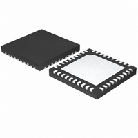
IC TXRX IEEE/ZIGBEE 2.4GHZ 40QFN
Manufacturer
Microchip Technology
Specifications of MRF24J40-I/ML
Package / Case
40-QFN
Frequency
2.4GHz
Data Rate - Maximum
250kbps
Modulation Or Protocol
802.15.4
Applications
ISM, ZigBee™
Power - Output
0dBm
Sensitivity
-95dBm
Voltage - Supply
2.4 V ~ 3.6 V
Current - Receiving
18mA
Current - Transmitting
18mA
Data Interface
PCB, Surface Mount
Antenna Connector
PCB, Surface Mount
Operating Temperature
-40°C ~ 85°C
Number Of Receivers
1
Number Of Transmitters
1
Wireless Frequency
2.4 GHz
Interface Type
4 Wire SPI
Noise Figure
8 dB
Output Power
+ 0 dBm
Operating Supply Voltage
2.5 V, 3.3 V
Maximum Operating Temperature
85 C
Mounting Style
SMD/SMT
Maximum Supply Current
22 mA
Minimum Operating Temperature
- 40 C
Lead Free Status / RoHS Status
Lead free / RoHS Compliant
Memory Size
-
Lead Free Status / Rohs Status
Lead free / RoHS Compliant
Available stocks
Company
Part Number
Manufacturer
Quantity
Price
Company:

Part Number:
MRF24J40-I/ML
Manufacturer:
MICROCHIP
Quantity:
12 000
Part Number:
MRF24J40-I/ML
Manufacturer:
MICROCHIP/微芯
Quantity:
20 000


2.4
Recommended bypass capacitors are listed in
Table 2-2. V
capacitors to ensure sufficient bypass decoupling. Min-
imize trace length from the V
capacitors and make them as short as possible.
TABLE 2-2:
2.5
The 20 MHz main oscillator provides the main
frequency (MAINCLK) signal to internal RF, baseband
and MAC circuitry. An external 20 MHz quartz crystal is
connected to the OSC1 and OSC2 pins as shown in
Figure 2-2. The crystal parameters are listed in
Table 2-3.
TABLE 2-3:
DS39776C-page 10
MRF24J40
Frequency
Frequency Tolerance at 25°C
Frequency Stability over Operating
Temperature Range
Mode
Load Capacitance
ESR
Note 1:
V
DD
21
31
32
35
37
39
1
4
5
2:
Pin
Power and Ground Pins
20 MHz Main Oscillator
These values are for design guidance only.
IEEE 802.15.4™ Standard specifies
transmitted center frequency tolerance
shall be ±40 ppm maximum.
DD
Parameter
pins 1 and 31 require two bypass
RECOMMENDED BYPASS
CAPACITOR VALUES
20 MHz CRYSTAL
PARAMETERS
Bypass Capacitor
47 pF and 0.01 μF
47 pF and 0.01 μF
0.01 μF
0.01 μF
0.1 μF
47 pF
47 pF
47 pF
DD
1 μF
pin to the bypass
(1)
Fundamental
±20 ppm
±20 ppm
80Ω max.
10-15 pF
20 MHz
Value
(2)
(2)
Preliminary
counters. The Sleep mode counters time the Beacon
information.
FIGURE 2-2:
2.6
The Phase-Locked Loop (PLL) circuitry requires one
external capacitor connected to pin 40 (LCAP). The
recommended value is 100 pF. The PCB layout around
the capacitor and pin 40 should be designed carefully
such as to minimize interference to the PLL.
2.7
The 32 kHz external crystal oscillator provides one of two
Sleep clock (SLPCLK) frequencies to Sleep mode
Interval (BI) and inactive period for a beacon-enabled
device and the Sleep interval for a nonbeacon-enabled
device. Refer to Section 3.15 “Sleep” for more
The SLPCLK frequency is selectable between the 32
kHz external crystal oscillator or 100 kHz internal oscil-
lator. The 32 kHz external crystal oscillator provides
better frequency accuracy and stability than the 100
kHz internal oscillator. An external 32 kHz tuning fork
crystal is connected to the LPOSC1 and LPOSC2 pins,
as shown in Figure 2-3. The crystal parameters are
listed in Table 2-4.
TABLE 2-4:
Frequency
Frequency Tolerance
Load Capacitance
ESR
Note 1:
Parameter
Phase-Locked Loop
32 kHz External Crystal Oscillator
CL2
CL1
These values are for design guidance only.
32 kHz CRYSTAL
PARAMETERS
20 MHz MAIN
OSCILLATOR CRYSTAL
CIRCUIT
X1
© 2010 Microchip Technology Inc.
OSC2
OSC1
70 kΩ max.
(1)
32.768 kHz
±20 ppm
Main Oscillator
12.5 pF
Value
20 MHz
Related parts for MRF24J40-I/ML
Image
Part Number
Description
Manufacturer
Datasheet
Request
R

Part Number:
Description:
IEEE 802.15.4� 2.4 GHz RF Transceiver
Manufacturer:
MICROCHIP [Microchip Technology]
Datasheet:

Part Number:
Description:
Ieee 802.15.4? 2.4 Ghz Rf Transceiver
Manufacturer:
Microchip Technology Inc.
Datasheet:
Part Number:
Description:
Manufacturer:
Microchip Technology Inc.
Datasheet:
Part Number:
Description:
Manufacturer:
Microchip Technology Inc.
Datasheet:
Part Number:
Description:
Manufacturer:
Microchip Technology Inc.
Datasheet:
Part Number:
Description:
Manufacturer:
Microchip Technology Inc.
Datasheet:
Part Number:
Description:
Manufacturer:
Microchip Technology Inc.
Datasheet:
Part Number:
Description:
Manufacturer:
Microchip Technology Inc.
Datasheet:
Part Number:
Description:
Manufacturer:
Microchip Technology Inc.
Datasheet:
Part Number:
Description:
Manufacturer:
Microchip Technology Inc.
Datasheet: