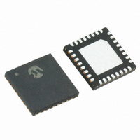
MRF89XA-I/MQ Microchip Technology, MRF89XA-I/MQ Datasheet - Page 81

MRF89XA-I/MQ
Manufacturer Part Number
MRF89XA-I/MQ
Description
TXRX ISM SUB-GHZ ULP 32QFN
Manufacturer
Microchip Technology
Specifications of MRF89XA-I/MQ
Package / Case
32-WFQFN Exposed Pad
Frequency
863MHz ~ 870MHz, 902MHz ~ 928MHz, 950MHz ~ 960MHz
Data Rate - Maximum
200kbps
Modulation Or Protocol
FSK, OOK
Applications
ISM
Power - Output
12.5dBm
Sensitivity
-113dBm
Voltage - Supply
2.1 V ~ 3.6 V
Current - Receiving
3mA
Current - Transmitting
25mA
Data Interface
PCB, Surface Mount
Antenna Connector
PCB, Surface Mount
Operating Temperature
-40°C ~ 85°C
Number Of Receivers
1
Number Of Transmitters
1
Wireless Frequency
863 MHz to 870 MHz, 902 MHz to 928 MHz, 950 MHz to 960 MHz
Interface Type
SPI
Noise Figure
- 112 dBc
Output Power
- 8.5 dBm, + 12.5 dBm
Operating Supply Voltage
2.1 V to 3.6 V
Maximum Operating Temperature
+ 85 C
Mounting Style
SMD/SMT
Maximum Data Rate
256 Kbps
Maximum Supply Current
25 mA
Minimum Operating Temperature
- 40 C
Modulation
FSK
Lead Free Status / RoHS Status
Lead free / RoHS Compliant
Memory Size
-
Lead Free Status / Rohs Status
Lead free / RoHS Compliant
Available stocks
Company
Part Number
Manufacturer
Quantity
Price
Company:
Part Number:
MRF89XA-I/MQ
Manufacturer:
MICROCHIP
Quantity:
12 000
3.10
In Buffered mode operation the NRZ data to/from the
(de)modulator is not directly accessed by the host
microcontroller but is stored in the FIFO and accessed
via the SPI data interface. This frees the host
microcontroller for other tasks between processing
data from the MRF89XA. Furthermore, it simplifies
software
microcontroller performance requirements (i.e., speed,
response). Note that in this mode the packet handler
stays inactive. The interface for Buffer mode is shown
in Figure 3-21.
An important feature is also the ability to empty the
FIFO in Stand-by mode, ensuring low power
consumption and adding greater software flexibility.
FIGURE 3-21:
© 2010 Microchip Technology Inc.
Note:
Data
Buffered Mode
Datapath
development
In this case Bit Synchronizer is automati-
cally enabled in Buffered mode. The Sync
word
(SYNCREN = 1) independently of the
FIFO filling method selected (FIFOFM).
TX
RX
Recognition
recognition
SYNC
BUFFERED MODE BLOCK DIAGRAM
overhead
must
and
be
MRF89XA
enabled
reduces
Preliminary
Control
(+SR)
FIFO
3.10.1
After entering TX in Buffered mode, the MRF89XA
expects the host microcontroller to write to the FIFO,
through the SPI data interface, all the data bytes to be
transmitted (preamble, Sync word, payload).
Actual transmission of the first byte will start either
when the FIFO is not empty (that is, first byte written by
the host microcontroller) or when the FIFO is full
depending on the IRQ0TXST bit (FTPRIREG<4>) set-
ting.
In Buffered mode the packet length is not limited, as
long as there are bytes inside the FIFO to be sent. When
the last byte is transferred to the SR, the FIFOEMPTY
IRQ
microcontroller, at that time the FIFO can still be filled
with additional bytes if required.
When the last bit of the last byte has left the Shift Reg-
ister (SR) (that is, eight bit periods later), the TXDONE
interrupt source is issued and the user can exit TX
mode after waiting at least one bit period from the last
bit processed by the modulator. If the transmitter is
switched OFF during transmission (for example, for
entering another chip mode), it will stop immediately,
even if there is still unsent data.
source
TX PROCESSING
is
CONFIG
DATA
issued
SPI
MRF89XA
to
interrupt
DS70622B-page 81
CSCON
SDO
SCK
SDI
IRQ1
CSDAT
IRQ0
the
host


