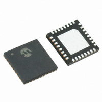
MRF89XA-I/MQ Microchip Technology, MRF89XA-I/MQ Datasheet - Page 23

MRF89XA-I/MQ
Manufacturer Part Number
MRF89XA-I/MQ
Description
TXRX ISM SUB-GHZ ULP 32QFN
Manufacturer
Microchip Technology
Specifications of MRF89XA-I/MQ
Package / Case
32-WFQFN Exposed Pad
Frequency
863MHz ~ 870MHz, 902MHz ~ 928MHz, 950MHz ~ 960MHz
Data Rate - Maximum
200kbps
Modulation Or Protocol
FSK, OOK
Applications
ISM
Power - Output
12.5dBm
Sensitivity
-113dBm
Voltage - Supply
2.1 V ~ 3.6 V
Current - Receiving
3mA
Current - Transmitting
25mA
Data Interface
PCB, Surface Mount
Antenna Connector
PCB, Surface Mount
Operating Temperature
-40°C ~ 85°C
Number Of Receivers
1
Number Of Transmitters
1
Wireless Frequency
863 MHz to 870 MHz, 902 MHz to 928 MHz, 950 MHz to 960 MHz
Interface Type
SPI
Noise Figure
- 112 dBc
Output Power
- 8.5 dBm, + 12.5 dBm
Operating Supply Voltage
2.1 V to 3.6 V
Maximum Operating Temperature
+ 85 C
Mounting Style
SMD/SMT
Maximum Data Rate
256 Kbps
Maximum Supply Current
25 mA
Minimum Operating Temperature
- 40 C
Modulation
FSK
Lead Free Status / RoHS Status
Lead free / RoHS Compliant
Memory Size
-
Lead Free Status / Rohs Status
Lead free / RoHS Compliant
Available stocks
Company
Part Number
Manufacturer
Quantity
Price
Company:
Part Number:
MRF89XA-I/MQ
Manufacturer:
MICROCHIP
Quantity:
12 000
Both of these SPIs are configured in Slave mode while
the host microcontroller is configured as the master.
They have separate selection pins (CSCON and
CSDAT) but share the remaining pins:
• SCK (SPI Clock): Clock signal provided by the
• SDI (SPI Input): Data Input signal provided by the
• SDO (SPI Output): Data Output signal provided
As listed in Table 2-5, only one interface can be
selected at a time with CSCON having the priority:
TABLE 2-5:
All the parameters can be programmed and set through
the SPI module. Any of these auxiliary functions can be
disabled when not required. After power-on, all param-
eters are set to default values. The programmed values
are retained during Sleep mode. The interface supports
the read out of a status register, which provides
detailed information about the status of the transceiver
and the received data.
© 2010 Microchip Technology Inc.
host microcontroller
host microcontroller
by the MRF89XA
CSDAT
0
0
1
1
CONFIG VS. DATA SPI
SELECTION
CSCON
0
1
0
1
CONFIG
CONFIG
DATA
None
SPI
Preliminary
The MRF89XA supports SPI mode 0,0, which requires
the SCK to remain idle in a low state. The CS pins,
/CSCON and /CSDAT based on the mode (pin 14 and
15), must be held low to enable communication
between the host microcontroller and the MRF89XA.
The device’s timing specification details are listed in
Table 5-7. The SDO pin defaults to a high impedance
(hi-Z) state when any of the CS pins are high (the
MRF89XA is not selected). This pin has a tri-state buf-
fer and uses a bus hold logic.
As the device uses byte writes, any of the Chip Select
(CS) pins should be pulled low for 8 bits. Data bits on
the SDI pin (pin 17) are shifted into the device upon the
rising edge of the clock on the SCK pin (pin 18) when-
ever the CS pins are low. The maximum clock fre-
quency for the SPI clock for CONFIG mode is 6 MHz.
However, maximum SPI Clock for DATA mode (to
read/write FIFO) is 1 MHz. Data is received by the
transceiver through the SDI pin and is clocked on the
rising edge of SCK. The MRF89XA sends the data
through the SDO pin and is clocked out on the falling
edge of SCK. The Most Significant bit (MSb) is sent first
in any data.
The SPI sequence diagrams are illustrated in
Figure 2-12 through Figure 2-15.
MRF89XA
DS70622B-page 23


