MRF89XA-I/MQ Microchip Technology, MRF89XA-I/MQ Datasheet
MRF89XA-I/MQ
Specifications of MRF89XA-I/MQ
Available stocks


Related parts for MRF89XA-I/MQ

MRF89XA-I/MQ Summary of contents
Page 1
... Ultra Low-Power, Integrated ISM Band 2010 Microchip Technology Inc. Sub-GHz Transceiver Advance Information MRF89XA Data Sheet DS70622A ...
Page 2
... REAL ICE, rfLAB, Select Mode, Total Endurance, TSHARC, UniWinDriver, WiperLock and ZENA are trademarks of Microchip Technology Incorporated in the U.S.A. and other countries. SQTP is a service mark of Microchip Technology Incorporated in the U.S.A. All other trademarks mentioned herein are property of their respective companies. ...
Page 3
... Sports and performance monitoring • Wireless toy controls • Medical applications General Description The MRF89XA is a single chip FSK/OOK trans- ceiver capable of operating in the 863-870 MHz and 902-928 MHz license-free ISM frequency bands, as well as the 950-960 MHz frequency band. The low- cost MRF89XA is optimized for very low-power consumption ( Receiver mode) ...
Page 4
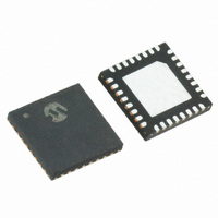
... MRF89XA Pin Diagram The following diagram shows the top view pin arrangement of the 32-pin QFN package. FIGURE 1: MRF89XA 32-PIN QFN PIN DIAGRAM 32-Pin QFN 32 TEST5 1 TEST1 2 VCORS 3 VCOTM 4 VCOTP 5 PLLM 6 PLLP 7 TEST6 8 9 Note 1: Pin 33 (GND) is located on the underside of the IC package. ...
Page 5
... When contacting a sales office, please specify which device, revision of silicon and data sheet (include literature number) you are using. Customer Notification System Register on our web site at www.microchip.com to receive the most current information on all of our products. 2010 Microchip Technology Inc. Advance Information MRF89XA DS70622A-page 5 ...
Page 6
... MRF89XA NOTES: DS70622A-page 6 Advance Information 2010 Microchip Technology Inc. ...
Page 7
... The MRF89XA supports a stable sensitivity and linearity characteristics for a wide supply range and is internally regulated. The frequency synthesizer of the MRF89XA is a fully integrated integer-N type PLL. The PLL circuit requires only five external components for the PLL loop filter and the VCO tank circuit. The PLL ...
Page 8
... FIGURE 1-1: MRF89XA SIMPLIFIED FUNCTIONAL BLOCK DIAGRAM Antenna Matching Saw Circuitry Filter Block Loop Tank Filter Circuit Block Block MRF89XA RF Block PARS Baseband Data RFIO Amplifier/ RF Parts Processing Filter/ Unit Limiter Power Memory Management Crystal Frequency = 12.8 MHz ® PIC MCU ...
Page 9
... HARDWARE DESCRIPTION The MRF89XA is an integrated, single chip, low-power ISM band sub-GHz transceiver. A simplified architec- tural block diagram of the MRF89XA is shown in Figure 2-1. The frequency synthesizer is clocked by an external 12.8 crystal, and frequency ranges from 863-870 MHz, 902-928 MHz and 950-960 MHz. ...
Page 10
... FIGURE 2-1: MRF89XA BLOCK DIAGRAM Reception Block First LNA Stage Mixers LO1 RX RFIO X LO1 TX I Second PA Stage Mixers Q Transmission Block Supply Block x x Supply RSSI I Second Filtering/ Stage IF Gain Amplification Mixers Q LO2 RX LO2 TX I Modulation First (DDS, DACs, Stage Interpolation Filters) ...
Page 11
... Analog Input 12 TEST0 Digital Input 13 TEST8 Digital I/O 14 CSCON Digital Input 15 CSDATA Digital Input 16 SDO Digital Output Serial data output interface from MRF89XA. 17 SDI Digital Input 18 SCK Digital Input 19 CLKOUT Digital Output Clock output. 20 DATA Digital I/O 21 IRQ0 Digital Output Interrupt request output (‘0’). ...
Page 12
... FIGURE 2-2: APPLICATION CIRCUIT SCHEMATIC C2 PCB Antenna SAW Filter C12 IN OUT V BAT C1 TEST3 AVRS DVRS PARS Z – Match L3 TEST4 RFIO SPI Bus To Host MCU SDO GND CSDATA CSCON TEST8 MRF89XA TEST0 OSC2 OSC1 TEST7 VCO Tank Loop Filter Crystal ...
Page 13
... Memory Map for MRF89XA Configuration/Control/Status Registers The memory in the MRF89XA transceiver is imple- mented as static RAM and is accessible via the SPI port. Each memory location functionally addresses the command, control, status or data/FIFO fields as shown in Table 2-2 and Table 2-3. The control registers provide ...
Page 14
... MRF89XA TABLE 2-2: CONFIGURATION/CONTROL/STATUS REGISTER DESCRIPTION (CONTINUED) Receiver Parameters Configuration Registers: Size – 6 Bytes, Start Address – 16 Register Register Sl. No. Address Name 17. 16 FILCONREG 18. 17 PFCONREG 19. 18 SYNCREG 20. 19 RESVREG 21. 20 RSTSREG 22. 21 OOKCREG Sync Word Parameters Configuration Registers: Size – 4 Bytes, Start Address – 22 ...
Page 15
... Microchip Technology Inc. Register Description Payload Configuration Register Node Address Set Register Packet Configuration Register FIFO CRC Configuration Register Advance Information MRF89XA Related Control Functions Enable Manchester encoding/decoding, payload length Node’s local address for filtering of received packets Packet format, size of the preamble, ...
Page 16
TABLE 2-3: CONFIGURATION/CONTROL/STATUS REGISTER MAP Register Function/ Register Register Name Bit 7 Parameter Address Type General 0 GCONREG CMOD2 1 DMODREG MODSEL1 2 FDEVREG FDVAL7 3 BRSREG Reserved 4 FLTHREG FTOVAL7 5 FIFOCREG FSIZE1 6 R1CNTSREG R1CVAL7 7 P1CNTSREG P1CVAL7 ...
Page 17
... This is a stress rating only and functional operation of the device at those or any other conditions above those indicated in the operation listings of this specification is not implied. Exposure to maximum rating conditions for extended periods may affect device reliability. 2010 Microchip Technology Inc. (except RFIO and V SS (1) ............................................................................................... -0.3V to 3.7V ).......................................................................................... - Advance Information MRF89XA ) ....... -0. 0.3V DS70622A-page 17 ...
Page 18
... MRF89XA 3.1 ESD Notice The MRF89XA is a high-performance radio frequency device. It satisfies: • Class II of the JEDEC standard JESD22-A114-B (Human Body Model KV, except on all of the RF pins where it satisfies Class 1A. • Class III of the JEDEC standard JESD22-C101C (Charged Device Model) on all pins. ...
Page 19
... MHz step — 250 — µs 5 MHz step — 260 — µs 7 MHz step — 290 — µs 12 MHz step — 320 — µs 20 MHz step — 340 — µs 27 MHz step Advance Information MRF89XA Unit Condition V — V — µ µ 3 — Condition — ...
Page 20
... MRF89XA TABLE 3-5: RECEIVER AC CHARACTERISTICS Parameter Sensitivity (FSK) Sensitivity (OOK) Co-Channel Rejection Adjacent Channel Rejection Blocking Immunity Receiver Bandwidth in FSK (2) Mode Receiver Bandwidth in OOK (2) Mode Input Third Order Intercept Point Receiver Wake-up Time Receiver Wake-up Time Receiver Hop Time from RX Ready to RX Ready with a ...
Page 21
... MHz, unless otherwise specified. DD Advance Information MRF89XA Condition Maximum power setting. Minimum power setting. Measured with a 600 kHz offset at the transmitter output. At any offset between 200 kHz and 600 kHz, unmodulated carrier, Fdev = 50 kHz. ...
Page 22
... MRF89XA NOTES: DS70622A-page 22 Advance Information 2010 Microchip Technology Inc. ...
Page 23
... APPENDIX A: REVISION HISTORY Revision A (January 2010) This is the initial released version of this document. 2010 Microchip Technology Inc. Advance Information MRF89XA DS70622A-page 23 ...
Page 24
... MRF89XA NOTES: DS70622A-page 24 Advance Information 2010 Microchip Technology Inc. ...
Page 25
... Local sales offices are also available to help customers. A listing of sales offices and locations is included in the back of this document. Technical support is available through the web site at: http://support.microchip.com Advance Information MRF89XA MRF89XA should contact their distributor, DS70622A-page 25 ...
Page 26
... Telephone: (_______) _________ - _________ Application (optional): Would you like a reply? Y Device: MRF89XA Questions: 1. What are the best features of this document? 2. How does this document meet your hardware and software development needs you find the organization of this document easy to follow? If not, why? 4 ...
Page 27
... MRF89XA: Ultra Low-Power, Integrated ISM Band Sub-GHz Transceiver Temperature I = -40ºC to +85ºC (Industrial) Range Package MQ = QFN (Quad Flat, No Lead Tape and Reel 2010 Microchip Technology Inc. Example: XXX a) Pattern b) Advance Information MRF89XA . MRF89XA-I/MQ: Industrial temperature, QFN package. MRF89XAT-I/MQ: Industrial temperature, QFN package, tape and reel. DS70622A-page 27 ...
Page 28
... France - Paris Tel: 33-1-69-53-63-20 Fax: 33-1-69-30-90-79 Germany - Munich Tel: 49-89-627-144-0 Fax: 49-89-627-144-44 Italy - Milan Tel: 39-0331-742611 Fax: 39-0331-466781 Netherlands - Drunen Tel: 31-416-690399 Fax: 31-416-690340 Spain - Madrid Tel: 34-91-708-08-90 Fax: 34-91-708-08- Wokingham Tel: 44-118-921-5869 Fax: 44-118-921-5820 01/05/10 2010 Microchip Technology Inc. ...