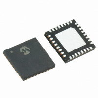
MRF89XA-I/MQ Microchip Technology, MRF89XA-I/MQ Datasheet - Page 28

MRF89XA-I/MQ
Manufacturer Part Number
MRF89XA-I/MQ
Description
TXRX ISM SUB-GHZ ULP 32QFN
Manufacturer
Microchip Technology
Specifications of MRF89XA-I/MQ
Package / Case
32-WFQFN Exposed Pad
Frequency
863MHz ~ 870MHz, 902MHz ~ 928MHz, 950MHz ~ 960MHz
Data Rate - Maximum
200kbps
Modulation Or Protocol
FSK, OOK
Applications
ISM
Power - Output
12.5dBm
Sensitivity
-113dBm
Voltage - Supply
2.1 V ~ 3.6 V
Current - Receiving
3mA
Current - Transmitting
25mA
Data Interface
PCB, Surface Mount
Antenna Connector
PCB, Surface Mount
Operating Temperature
-40°C ~ 85°C
Number Of Receivers
1
Number Of Transmitters
1
Wireless Frequency
863 MHz to 870 MHz, 902 MHz to 928 MHz, 950 MHz to 960 MHz
Interface Type
SPI
Noise Figure
- 112 dBc
Output Power
- 8.5 dBm, + 12.5 dBm
Operating Supply Voltage
2.1 V to 3.6 V
Maximum Operating Temperature
+ 85 C
Mounting Style
SMD/SMT
Maximum Data Rate
256 Kbps
Maximum Supply Current
25 mA
Minimum Operating Temperature
- 40 C
Modulation
FSK
Lead Free Status / RoHS Status
Lead free / RoHS Compliant
Memory Size
-
Lead Free Status / Rohs Status
Lead free / RoHS Compliant
Available stocks
Company
Part Number
Manufacturer
Quantity
Price
Company:
Part Number:
MRF89XA-I/MQ
Manufacturer:
MICROCHIP
Quantity:
12 000
2.12
In Buffered and Packet modes of operation, data to be
transmitted and data that has been received are stored
in a configurable First In First Out (FIFO) buffer. The
FIFO is accessed through the SPI data interface and
provides several interrupts for transfer management.
The FIFO is 1 byte (8 bits) wide; therefore, it only
performs byte (parallel) operations, whereas the
demodulator functions serially. A shift register (SR) is
therefore employed to interface the demodulator and
the FIFO. In Transmit mode it takes bytes from the
FIFO and outputs them serially (MSB first) at the
programmed bit rate to the modulator. Similarly, in
Receive mode the shift register gets bit-by-bit data from
the demodulator and writes them byte-by-byte to the
FIFO. This is illustrated in Figure 2-16.
FIGURE 2-16:
FIGURE 2-17:
DS70622B-page 28
MRF89XA
Data TX/RX
FIFO and Shift Register (SR)
1
0x00
0x1F
MSB
FIFO AND SHIFT
REGISTER
MRF89XA MEMORY SPACE
SR (8 bits)
Byte 0
Byte 1
Control Registers
8
Data TX/RX
LSB
FIFO
1
Preliminary
0x40
0x00
MSB
2.13
The memory in the MRF89XA transceiver is
implemented as static RAM and is accessible through
the SPI port. The memory configuration of the
MRF89XA is illustrated in Figure 2-17 and Figure 2-18.
SHIFT REGISTER
Transmit/Receive
MRF89XAConfiguration/Control/
Status Registers
(8 bits)
FIFO
© 2010 Microchip Technology Inc.
64 bytes


