MRF89XA-I/MQ Microchip Technology, MRF89XA-I/MQ Datasheet - Page 105
MRF89XA-I/MQ
Manufacturer Part Number
MRF89XA-I/MQ
Description
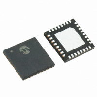
TXRX ISM SUB-GHZ ULP 32QFN
Manufacturer
Microchip Technology
Specifications of MRF89XA-I/MQ
Package / Case
32-WFQFN Exposed Pad
Frequency
863MHz ~ 870MHz, 902MHz ~ 928MHz, 950MHz ~ 960MHz
Data Rate - Maximum
200kbps
Modulation Or Protocol
FSK, OOK
Applications
ISM
Power - Output
12.5dBm
Sensitivity
-113dBm
Voltage - Supply
2.1 V ~ 3.6 V
Current - Receiving
3mA
Current - Transmitting
25mA
Data Interface
PCB, Surface Mount
Antenna Connector
PCB, Surface Mount
Operating Temperature
-40°C ~ 85°C
Number Of Receivers
1
Number Of Transmitters
1
Wireless Frequency
863 MHz to 870 MHz, 902 MHz to 928 MHz, 950 MHz to 960 MHz
Interface Type
SPI
Noise Figure
- 112 dBc
Output Power
- 8.5 dBm, + 12.5 dBm
Operating Supply Voltage
2.1 V to 3.6 V
Maximum Operating Temperature
+ 85 C
Mounting Style
SMD/SMT
Maximum Data Rate
256 Kbps
Maximum Supply Current
25 mA
Minimum Operating Temperature
- 40 C
Modulation
FSK
Lead Free Status / RoHS Status
Lead free / RoHS Compliant
Memory Size
-
Lead Free Status / Rohs Status
Lead free / RoHS Compliant
Available stocks
Company
Part Number
Manufacturer
Quantity
Price
Company:

Part Number:
MRF89XA-I/MQ
Manufacturer:
MICROCHIP
Quantity:
12 000


4.8
The following guidelines can be used to assist in
high-frequency PCB layout design.
The printed circuit board is usually comprised of two or
four basic FR4 layers.
The two-layer printed circuit board has mixed sig-
nal/power/RF and common ground routed in both the
layers (see Figure 4-8).
The four-layer printed circuit board (see Figure 4-9) is
comprised of the following layers:
• Signal layout
• RF ground
• Power line routing
• Common ground
The following guidelines explain the requirements of
the previously mentioned layers:
• It is important to keep the original PCB thickness,
• For good transmit and receive performance, the
• Except for the antenna layout, avoid sharp corners
• Digital lines are prone to be very noisy when han-
• A VIA filled ground patch underneath the IC
• The power supply must be distributed to each pin in
FIGURE 4-8:
© 2010 Microchip Technology Inc.
because any change will affect antenna perfor-
mance (see total thickness of dielectric) or
microstrip lines’ characteristic impedance.
trace lengths at the RF pins must be kept as short
as possible. Using small, surface mount compo-
nents (in 0402/0603 package) yields good perfor-
mance and keeps the RF circuit small. RF
connections should be short and direct.
because they can act as an antenna. Round corners
will eliminate possible future EMI problems.
dling periodic waveforms and fast clock/switching
rates. Avoid RF signal layout close to any of the
digital lines.
transceiver is mandatory.
a star topology, and low-ESR capacitors must be
placed at each pin for proper decoupling noise.
General PCB Layout Design
TWO BASIC COPPER FR4 LAYERS
Preliminary
• Thorough decoupling on each power pin is
• Passive component (inductors) should be in the
• The additional trace length affects the crystal
• Setting short and direct connections between the
• Long run tracks of clock signal may radiate and
• Keep clock connections as short as possible and
• Low value decoupling capacitors, typically 0.01-0.1
• High value decoupling capacitors, typically 2.2-10
• Power supply bypassing is necessary. Poor bypass-
beneficial for reducing in-band transceiver noise,
particularly when this noise degrades performance.
Usually, low value caps (27-47 pF) combined with
large value caps (100 nF) will cover a large
spectrum of frequency.
high-frequency category and the Self-Resonant
Frequency (SRF) should be at least two times
higher than the operating frequency.
oscillator by adding parasitic capacitance to the
overall load of the crystal. To minimize this, place
the crystal as close as possible to the RF device.
components on board minimizes the effects of
“frequency pulling” that might be introduced by stray
capacitance. It even allows the internal load capaci-
tance of the chip to be more effective in properly
loading the crystal oscillator circuit.
cause interference. This can degrade receiver per-
formance and add harmonics or unwanted
modulation to the transmitter.
surround the clock trace with an adjacent ground
plane pour. Pouring helps in reducing any radiation
or crosstalk due to long run traces of the clock
signal.
µF, should be placed for V
points of the RF circuit.
µF, should be placed at the point where power is
applied to the PCB.
ing contributes to conducted interference, which can
cause noise and spurious signals to couple into the
RF sections, significantly reducing the performance.
Signal/Power/RF and
Common Ground
Dielectric Constant = 4.5
Signal/Power/RF and
Common Ground
DD
MRF89XA
of the chip and for bias
DS70622B-page 105
Related parts for MRF89XA-I/MQ
Image
Part Number
Description
Manufacturer
Datasheet
Request
R

Part Number:
Description:
Ultra-low Power, Integrated Ism Band Sub-ghz Transceiver
Manufacturer:
Microchip Technology Inc.
Datasheet:
Part Number:
Description:
Manufacturer:
Microchip Technology Inc.
Datasheet:
Part Number:
Description:
Manufacturer:
Microchip Technology Inc.
Datasheet:
Part Number:
Description:
Manufacturer:
Microchip Technology Inc.
Datasheet:
Part Number:
Description:
Manufacturer:
Microchip Technology Inc.
Datasheet:
Part Number:
Description:
Manufacturer:
Microchip Technology Inc.
Datasheet:
Part Number:
Description:
Manufacturer:
Microchip Technology Inc.
Datasheet:
Part Number:
Description:
Manufacturer:
Microchip Technology Inc.
Datasheet:
Part Number:
Description:
Manufacturer:
Microchip Technology Inc.
Datasheet: