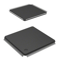
HD6417706F133 Renesas Electronics America, HD6417706F133 Datasheet - Page 604

HD6417706F133
Manufacturer Part Number
HD6417706F133
Description
IC SUPERH MPU ROMLESS 176LQFP
Manufacturer
Renesas Electronics America
Series
SuperH® SH7700r
Datasheet
1.HD6417706F133V.pdf
(751 pages)
Specifications of HD6417706F133
Core Processor
SH-3
Core Size
32-Bit
Speed
133MHz
Connectivity
EBI/EMI, FIFO, SCI, SmartCard
Peripherals
DMA, POR, WDT
Number Of I /o
103
Program Memory Type
ROMless
Ram Size
16K x 8
Voltage - Supply (vcc/vdd)
1.75 V ~ 2.05 V
Oscillator Type
Internal
Operating Temperature
-20°C ~ 75°C
Package / Case
176-LQFP
Lead Free Status / RoHS Status
Contains lead / RoHS non-compliant
Eeprom Size
-
Program Memory Size
-
Data Converters
-
Available stocks
Company
Part Number
Manufacturer
Quantity
Price
Part Number:
HD6417706F133
Manufacturer:
RENESAS/瑞萨
Quantity:
20 000
Company:
Part Number:
HD6417706F133V
Manufacturer:
EDISON
Quantity:
2 000
Company:
Part Number:
HD6417706F133V
Manufacturer:
Renesas Electronics America
Quantity:
10 000
Part Number:
HD6417706F133V
Manufacturer:
RENESAS/瑞萨
Quantity:
20 000
- Current page: 604 of 751
- Download datasheet (5Mb)
Section 21 User Debugging Interface (H-UDI)
21.1
The H-UDI has the following features.
21.2
Table 21.1 lists the pin configuration of the H-UDI.
Table 21.1 Pin Configuraiton
Name
TCK
TMS
TRST
TDI
TDO
ASEMD0
ASEBRKAK
Rev. 5.00 May 29, 2006 page 554 of 698
REJ09B0146-0500
Support of the E10A emulator
Standard pin arrangement of JTAG
Real-time branch trace
1-kbyte on-chip RAM for running the high-speed emulation program
Input/Output Pin
Feature
Description
H-UDI serial data input/output clock pin. Data is serially supplied to the H-UDI from
the data input pin (TDI), and output from the data output pin (TDO), in
synchronization with this clock.
Mode select input pin. The state of the TAP control circuit is determined by
changing this signal in synchronization with TCK. The protocol conforms to the
JTAG standard (IEEE Std. 1149.1).
H-UDI reset input pin. Input is accepted asynchronously with respect to TCK, and
when low, the H-UDI is reset. See section 21.4.2, Reset Configuration, for more
information.
H-UDI serial data input pin. Data transfer to the H-UDI is executed by changing this
signal in synchronization with TCK.
H-UDI serial data output pin. Data output from the H-UDI is executed by reading
this signal in synchronization with TCK.
ASE mode select pin. If a low level is input at the ASEMD0 pin while the RESETP
pin is asserted, ASE mode is entered; if a high level is input, normal operation
mode is entered. ASEMD0 pin should be high level when an emulator or H-UDI is
not used. In ASE mode, boundary scan and emulator functions can be used. The
input level at the ASEMD0 pin should be held for at least one cycle after RESETP
negation.
Dedicated emulator pin
Related parts for HD6417706F133
Image
Part Number
Description
Manufacturer
Datasheet
Request
R

Part Number:
Description:
KIT STARTER FOR M16C/29
Manufacturer:
Renesas Electronics America
Datasheet:

Part Number:
Description:
KIT STARTER FOR R8C/2D
Manufacturer:
Renesas Electronics America
Datasheet:

Part Number:
Description:
R0K33062P STARTER KIT
Manufacturer:
Renesas Electronics America
Datasheet:

Part Number:
Description:
KIT STARTER FOR R8C/23 E8A
Manufacturer:
Renesas Electronics America
Datasheet:

Part Number:
Description:
KIT STARTER FOR R8C/25
Manufacturer:
Renesas Electronics America
Datasheet:

Part Number:
Description:
KIT STARTER H8S2456 SHARPE DSPLY
Manufacturer:
Renesas Electronics America
Datasheet:

Part Number:
Description:
KIT STARTER FOR R8C38C
Manufacturer:
Renesas Electronics America
Datasheet:

Part Number:
Description:
KIT STARTER FOR R8C35C
Manufacturer:
Renesas Electronics America
Datasheet:

Part Number:
Description:
KIT STARTER FOR R8CL3AC+LCD APPS
Manufacturer:
Renesas Electronics America
Datasheet:

Part Number:
Description:
KIT STARTER FOR RX610
Manufacturer:
Renesas Electronics America
Datasheet:

Part Number:
Description:
KIT STARTER FOR R32C/118
Manufacturer:
Renesas Electronics America
Datasheet:

Part Number:
Description:
KIT DEV RSK-R8C/26-29
Manufacturer:
Renesas Electronics America
Datasheet:

Part Number:
Description:
KIT STARTER FOR SH7124
Manufacturer:
Renesas Electronics America
Datasheet:

Part Number:
Description:
KIT STARTER FOR H8SX/1622
Manufacturer:
Renesas Electronics America
Datasheet:

Part Number:
Description:
KIT DEV FOR SH7203
Manufacturer:
Renesas Electronics America
Datasheet:


