PIC18C242/JW Microchip Technology, PIC18C242/JW Datasheet - Page 89
PIC18C242/JW
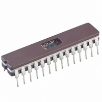
Manufacturer Part Number
PIC18C242/JW
Description
IC MCU EPROM 8KX16 A/D 28CDIP
Manufacturer
Microchip Technology
Series
PIC® 18Cr
Datasheets
1.PIC16F616T-ISL.pdf
(8 pages)
2.PIC16C770-ISO.pdf
(8 pages)
3.PIC18C242-ISO.pdf
(305 pages)
4.PIC18C242-ISO.pdf
(12 pages)
Specifications of PIC18C242/JW
Core Processor
PIC
Core Size
8-Bit
Speed
40MHz
Connectivity
I²C, SPI, UART/USART
Peripherals
Brown-out Detect/Reset, LVD, POR, PWM, WDT
Number Of I /o
22
Program Memory Size
16KB (8K x 16)
Program Memory Type
EPROM, UV
Ram Size
512 x 8
Voltage - Supply (vcc/vdd)
4.2 V ~ 5.5 V
Data Converters
A/D 5x10b
Oscillator Type
External
Operating Temperature
0°C ~ 70°C
Package / Case
28-CDIP (0.300", 7.62mm) Window
Lead Free Status / RoHS Status
Contains lead / RoHS non-compliant
Eeprom Size
-
Available stocks
Company
Part Number
Manufacturer
Quantity
Price
Company:

Part Number:
PIC18C242/JW
Manufacturer:
NS
Quantity:
10


8.5
This section is only applicable to the PIC18C4X2
devices.
PORTE is a 3-bit wide, bi-directional port. The corre-
sponding Data Direction register is TRISE. Setting a
TRISE bit (= 1) will make the corresponding PORTE pin
an input (i.e., put the corresponding output driver in a
Hi-Impedance mode). Clearing a TRISE bit (= 0) will
make the corresponding PORTE pin an output (i.e., put
the contents of the output latch on the selected pin).
The Data Latch register (LATE) is also memory
mapped. Read-modify-write operations on the LATE
register reads and writes the latched output value for
PORTE.
PORTE has three pins (RE0/RD/AN5, RE1/WR/AN6
and RE2/CS/AN7), which are individually configurable
as inputs or outputs. These pins have Schmitt Trigger
input buffers.
Register 8-1 shows the TRISE register, which also con-
trols the parallel slave port operation.
PORTE pins are multiplexed with analog inputs. When
selected as an analog input, these pins will read as ’0’s.
TRISE controls the direction of the RE pins, even when
they are being used as analog inputs. The user must
make sure to keep the pins configured as inputs when
using them as analog inputs.
EXAMPLE 8-5:
CLRF
CLRF
MOVLW
MOVWF
MOVLW
MOVWF
Note:
Note:
2001 Microchip Technology Inc.
PORTE, TRISE and LATE
Registers
PORTE
LATE
0x07
ADCON1
0x03
TRISC
On a Power-on Reset, these pins are con-
figured as digital inputs.
On a Power-on Reset, these pins are con-
figured as analog inputs.
; Initialize PORTE by
; clearing output
; data latches
; Alternate method
; to clear output
; data latches
; Configure A/D
; for digital inputs
; Value used to
; initialize data
; direction
; Set RE<0> as inputs
; RE<1> as outputs
; RE<2> as inputs
INITIALIZING PORTE
FIGURE 8-9:
WR LATE
or
PORTE
WR TRISE
Note 1: I/O pins have diode protection to V
Data
Bus
RD PORTE
To Analog Converter
TRIS Latch
Data Latch
D
D
CK
CK
RD LATE
RD TRISE
Q
Q
PORTE BLOCK DIAGRAM
IN I/O PORT MODE
PIC18CXX2
Q
EN
EN
D
Schmitt
Trigger
Input
Buffer
DS39026C-page 87
DD
and V
SS
I/O pin
.
(1)
Related parts for PIC18C242/JW
Image
Part Number
Description
Manufacturer
Datasheet
Request
R

Part Number:
Description:
IC, 8BIT MCU, PIC18F, 40MHZ, LCC-44
Manufacturer:
Microchip Technology
Datasheet:
Part Number:
Description:
IC, 8BIT MCU, PIC18LF, 40MHZ, PLCC-64
Manufacturer:
Microchip Technology
Datasheet:
Part Number:
Description:
IC, 8BIT MCU, PIC18F, 64MHZ, TQFP-80
Manufacturer:
Microchip Technology
Datasheet:

Part Number:
Description:
MCU, MPU & DSP Development Tools CAN/LIN PICtail Plus Daughter Board
Manufacturer:
Microchip Technology
Datasheet:

Part Number:
Description:
IC, 8BIT MCU, PIC18F, 64MHZ, DIP-40
Manufacturer:
Microchip Technology
Datasheet:

Part Number:
Description:
IC, 8BIT MCU, PIC18LF, 40MHZ, PLCC-64
Manufacturer:
Microchip Technology
Datasheet:
Part Number:
Description:
IC, 8BIT MCU, PIC18F, 64MHZ, TQFP-64
Manufacturer:
Microchip Technology
Part Number:
Description:
IC, 8BIT MCU, PIC18F, 64MHZ, TQFP-80
Manufacturer:
Microchip Technology

Part Number:
Description:
8KB, Flash, 768bytes-RAM, 36I/O, 8-bit Family,nanowatt XLP 40 UQFN 5x5x0.5mm TUB
Manufacturer:
Microchip Technology
Datasheet:
Part Number:
Description:
8KB, Flash, 768bytes-RAM, 36I/O, 8-bit Family,nanowatt XLP 40 UQFN 5x5x0.5mm TUB
Manufacturer:
Microchip Technology
Part Number:
Description:
16KB, Flash, 768bytes-RAM, 36I/O, 8-bit Family,nanowatt XLP 40 UQFN 5x5x0.5mm TU
Manufacturer:
Microchip Technology
Datasheet:
Part Number:
Description:
16KB, Flash, 768bytes-RAM, 36I/O, 8-bit Family,nanowatt XLP 40 UQFN 5x5x0.5mm TU
Manufacturer:
Microchip Technology
Part Number:
Description:
32KB, Flash, 1536bytes-RAM, 36I/O, 8-bit Family,nanowatt XLP 40 UQFN 5x5x0.5mm T
Manufacturer:
Microchip Technology
Datasheet:
Part Number:
Description:
32KB, Flash, 1536bytes-RAM, 36I/O, 8-bit Family,nanowatt XLP 40 UQFN 5x5x0.5mm T
Manufacturer:
Microchip Technology
Part Number:
Description:
64KB, Flash, 3968bytes-RAM, 36I/O, 8-bit Family,nanowatt XLP 40 UQFN 5x5x0.5mm T
Manufacturer:
Microchip Technology
Datasheet: