PIC18C242/JW Microchip Technology, PIC18C242/JW Datasheet - Page 167
PIC18C242/JW
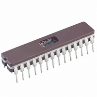
Manufacturer Part Number
PIC18C242/JW
Description
IC MCU EPROM 8KX16 A/D 28CDIP
Manufacturer
Microchip Technology
Series
PIC® 18Cr
Datasheets
1.PIC16F616T-ISL.pdf
(8 pages)
2.PIC16C770-ISO.pdf
(8 pages)
3.PIC18C242-ISO.pdf
(305 pages)
4.PIC18C242-ISO.pdf
(12 pages)
Specifications of PIC18C242/JW
Core Processor
PIC
Core Size
8-Bit
Speed
40MHz
Connectivity
I²C, SPI, UART/USART
Peripherals
Brown-out Detect/Reset, LVD, POR, PWM, WDT
Number Of I /o
22
Program Memory Size
16KB (8K x 16)
Program Memory Type
EPROM, UV
Ram Size
512 x 8
Voltage - Supply (vcc/vdd)
4.2 V ~ 5.5 V
Data Converters
A/D 5x10b
Oscillator Type
External
Operating Temperature
0°C ~ 70°C
Package / Case
28-CDIP (0.300", 7.62mm) Window
Lead Free Status / RoHS Status
Contains lead / RoHS non-compliant
Eeprom Size
-
Available stocks
Company
Part Number
Manufacturer
Quantity
Price
Company:

Part Number:
PIC18C242/JW
Manufacturer:
NS
Quantity:
10


16.0
The analog-to-digital (A/D) converter module has five
inputs for the PIC18C2x2 devices and eight for the
PIC18C4x2 devices. This module has the ADCON0
and ADCON1 register definitions that are compatible
with the mid-range A/D module.
The A/D allows conversion of an analog input signal to
a corresponding 10-bit digital number.
REGISTER 16-1:
2000 Microchip Technology Inc.
COMPATIBLE 10-BIT ANALOG-
TO-DIGITAL CONVERTER (A/D)
MODULE
bit 7-6
bit 5-3
bit 2
bit 1
bit 0
ADCON0 REGISTER
Legend:
R = Readable bit
- n = Value at POR reset
bit 7
ADCS1:ADCS0: A/D Conversion Clock Select bits (ADCON0 bits in bold
CHS2:CHS0: Analog Channel Select bits
000 = channel 0 (AN0)
001 = channel 1 (AN1)
010 = channel 2 (AN2)
011 = channel 3 (AN3)
100 = channel 4 (AN4)
101 = channel 5 (AN5)
110 = channel 6 (AN6)
111 = channel 7 (AN7)
Note:
GO/DONE: A/D Conversion Status bit
When ADON = 1:
1 = A/D conversion in progress (setting this bit starts the A/D conversion which is automatically
0 = A/D conversion not in progress
Unimplemented: Read as '0'
ADON: A/D On bit
1 = A/D converter module is powered up
0 = A/D converter module is shut-off and consumes no operating current
ADCS1
<ADCS2>
ADCON1
R/W-0
cleared by hardware when the A/D conversion is complete)
0
0
0
0
1
1
1
1
The PIC18C2X2 devices do not implement the full 8 A/D channels; the unimplemented selections
are reserved. Do not select any unimplemented channel.
<ADCS1:ADCS0>
ADCS0
R/W-0
ADCON0
00
01
10
11
00
01
10
11
R/W-0
CHS2
W = Writable bit
’1’ = Bit is set
F
F
F
F
F
F
F
F
OSC
OSC
OSC
RC
OSC
OSC
OSC
RC
(clock derived from the internal A/D RC oscillator)
(clock derived from the internal A/D RC oscillator)
/2
/8
/32
/4
/16
/64
R/W-0
CHS1
The A/D module has four registers. These registers
are:
• A/D Result High Register (ADRESH)
• A/D Result Low Register (ADRESL)
• A/D Control Register 0 (ADCON0)
• A/D Control Register 1 (ADCON1)
The ADCON0 register, shown in Register 16-1, con-
trols the operation of the A/D module. The ADCON1
register, shown in Register 16-2, configures the func-
tions of the port pins.
U = Unimplemented bit, read as ‘0’
’0’ = Bit is cleared
R/W-0
CHS0
Clock Conversion
GO/DONE
R/W-0
PIC18CXX2
)
x = Bit is unknown
DS39026C-page 165
U-0
—
R/W-0
ADON
bit 0
Related parts for PIC18C242/JW
Image
Part Number
Description
Manufacturer
Datasheet
Request
R

Part Number:
Description:
IC, 8BIT MCU, PIC18F, 40MHZ, LCC-44
Manufacturer:
Microchip Technology
Datasheet:
Part Number:
Description:
IC, 8BIT MCU, PIC18LF, 40MHZ, PLCC-64
Manufacturer:
Microchip Technology
Datasheet:
Part Number:
Description:
IC, 8BIT MCU, PIC18F, 64MHZ, TQFP-80
Manufacturer:
Microchip Technology
Datasheet:

Part Number:
Description:
MCU, MPU & DSP Development Tools CAN/LIN PICtail Plus Daughter Board
Manufacturer:
Microchip Technology
Datasheet:

Part Number:
Description:
IC, 8BIT MCU, PIC18F, 64MHZ, DIP-40
Manufacturer:
Microchip Technology
Datasheet:

Part Number:
Description:
IC, 8BIT MCU, PIC18LF, 40MHZ, PLCC-64
Manufacturer:
Microchip Technology
Datasheet:
Part Number:
Description:
IC, 8BIT MCU, PIC18F, 64MHZ, TQFP-64
Manufacturer:
Microchip Technology
Part Number:
Description:
IC, 8BIT MCU, PIC18F, 64MHZ, TQFP-80
Manufacturer:
Microchip Technology

Part Number:
Description:
8KB, Flash, 768bytes-RAM, 36I/O, 8-bit Family,nanowatt XLP 40 UQFN 5x5x0.5mm TUB
Manufacturer:
Microchip Technology
Datasheet:
Part Number:
Description:
8KB, Flash, 768bytes-RAM, 36I/O, 8-bit Family,nanowatt XLP 40 UQFN 5x5x0.5mm TUB
Manufacturer:
Microchip Technology
Part Number:
Description:
16KB, Flash, 768bytes-RAM, 36I/O, 8-bit Family,nanowatt XLP 40 UQFN 5x5x0.5mm TU
Manufacturer:
Microchip Technology
Datasheet:
Part Number:
Description:
16KB, Flash, 768bytes-RAM, 36I/O, 8-bit Family,nanowatt XLP 40 UQFN 5x5x0.5mm TU
Manufacturer:
Microchip Technology
Part Number:
Description:
32KB, Flash, 1536bytes-RAM, 36I/O, 8-bit Family,nanowatt XLP 40 UQFN 5x5x0.5mm T
Manufacturer:
Microchip Technology
Datasheet:
Part Number:
Description:
32KB, Flash, 1536bytes-RAM, 36I/O, 8-bit Family,nanowatt XLP 40 UQFN 5x5x0.5mm T
Manufacturer:
Microchip Technology
Part Number:
Description:
64KB, Flash, 3968bytes-RAM, 36I/O, 8-bit Family,nanowatt XLP 40 UQFN 5x5x0.5mm T
Manufacturer:
Microchip Technology
Datasheet: