PIC18C242/JW Microchip Technology, PIC18C242/JW Datasheet - Page 109
PIC18C242/JW
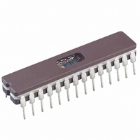
Manufacturer Part Number
PIC18C242/JW
Description
IC MCU EPROM 8KX16 A/D 28CDIP
Manufacturer
Microchip Technology
Series
PIC® 18Cr
Datasheets
1.PIC16F616T-ISL.pdf
(8 pages)
2.PIC16C770-ISO.pdf
(8 pages)
3.PIC18C242-ISO.pdf
(305 pages)
4.PIC18C242-ISO.pdf
(12 pages)
Specifications of PIC18C242/JW
Core Processor
PIC
Core Size
8-Bit
Speed
40MHz
Connectivity
I²C, SPI, UART/USART
Peripherals
Brown-out Detect/Reset, LVD, POR, PWM, WDT
Number Of I /o
22
Program Memory Size
16KB (8K x 16)
Program Memory Type
EPROM, UV
Ram Size
512 x 8
Voltage - Supply (vcc/vdd)
4.2 V ~ 5.5 V
Data Converters
A/D 5x10b
Oscillator Type
External
Operating Temperature
0°C ~ 70°C
Package / Case
28-CDIP (0.300", 7.62mm) Window
Lead Free Status / RoHS Status
Contains lead / RoHS non-compliant
Eeprom Size
-
Available stocks
Company
Part Number
Manufacturer
Quantity
Price
Company:

Part Number:
PIC18C242/JW
Manufacturer:
NS
Quantity:
10


13.0
Each CCP (Capture/Compare/PWM) module contains
a 16-bit register which can operate as a 16-bit capture
register, as a 16-bit compare register, or as a PWM
master/slave Duty Cycle register. Table 13-1 shows the
timer resources of the CCP module modes.
REGISTER 13-1:
2001 Microchip Technology Inc.
CAPTURE/COMPARE/PWM
(CCP) MODULES
bit 7-6
bit 5-4
bit 3-0
Legend:
R = Readable bit
- n = Value at POR reset
CCP1CON REGISTER/CCP2CON REGISTER
bit 7
Unimplemented: Read as '0'
DCxB1:DCxB0: PWM Duty Cycle bit1 and bit0
Capture mode:
Unused
Compare mode:
Unused
PWM mode:
These bits are the two LSbs (bit1 and bit0) of the 10-bit PWM duty cycle. The upper eight bits
(DCx9:DCx2) of the duty cycle are found in CCPRxL.
CCPxM3:CCPxM0: CCPx Mode Select bits
0000 = Capture/Compare/PWM off (resets CCPx module)
0001 = Reserved
0010 = Compare mode, toggle output on match (CCPxIF bit is set)
0011 = Reserved
0100 = Capture mode, every falling edge
0101 = Capture mode, every rising edge
0110 = Capture mode, every 4th rising edge
0111 = Capture mode, every 16th rising edge
1000 = Compare mode,
1001 = Compare mode,
1010 = Compare mode,
1011 = Compare mode,
11xx = PWM mode
U-0
—
Initialize CCP pin Low, on compare match force CCP pin High (CCPIF bit is set)
unaffected)
Initialize CCP pin High, on compare match force CCP pin Low (CCPIF bit is set)
Generate software interrupt on compare match (CCPIF bit is set, CCP pin is
Trigger special event (CCPIF bit is set)
U-0
—
DCxB1
R/W-0
W = Writable bit
’1’ = Bit is set
DCxB0
R/W-0
The operation of CCP1 is identical to that of CCP2, with
the exception of the special event trigger. Therefore,
operation of a CCP module in the following sections is
described with respect to CCP1.
Table 13-2 shows the interaction of the CCP modules.
CCPxM3
U = Unimplemented bit, read as ‘0’
’0’ = Bit is cleared
R/W-0
CCPxM2
R/W-0
PIC18CXX2
x = Bit is unknown
CCPxM1
R/W-0
DS39026C-page 107
CCPxM0
R/W-0
bit 0
Related parts for PIC18C242/JW
Image
Part Number
Description
Manufacturer
Datasheet
Request
R

Part Number:
Description:
IC, 8BIT MCU, PIC18F, 40MHZ, LCC-44
Manufacturer:
Microchip Technology
Datasheet:
Part Number:
Description:
IC, 8BIT MCU, PIC18LF, 40MHZ, PLCC-64
Manufacturer:
Microchip Technology
Datasheet:
Part Number:
Description:
IC, 8BIT MCU, PIC18F, 64MHZ, TQFP-80
Manufacturer:
Microchip Technology
Datasheet:

Part Number:
Description:
MCU, MPU & DSP Development Tools CAN/LIN PICtail Plus Daughter Board
Manufacturer:
Microchip Technology
Datasheet:

Part Number:
Description:
IC, 8BIT MCU, PIC18F, 64MHZ, DIP-40
Manufacturer:
Microchip Technology
Datasheet:

Part Number:
Description:
IC, 8BIT MCU, PIC18LF, 40MHZ, PLCC-64
Manufacturer:
Microchip Technology
Datasheet:
Part Number:
Description:
IC, 8BIT MCU, PIC18F, 64MHZ, TQFP-64
Manufacturer:
Microchip Technology
Part Number:
Description:
IC, 8BIT MCU, PIC18F, 64MHZ, TQFP-80
Manufacturer:
Microchip Technology

Part Number:
Description:
8KB, Flash, 768bytes-RAM, 36I/O, 8-bit Family,nanowatt XLP 40 UQFN 5x5x0.5mm TUB
Manufacturer:
Microchip Technology
Datasheet:
Part Number:
Description:
8KB, Flash, 768bytes-RAM, 36I/O, 8-bit Family,nanowatt XLP 40 UQFN 5x5x0.5mm TUB
Manufacturer:
Microchip Technology
Part Number:
Description:
16KB, Flash, 768bytes-RAM, 36I/O, 8-bit Family,nanowatt XLP 40 UQFN 5x5x0.5mm TU
Manufacturer:
Microchip Technology
Datasheet:
Part Number:
Description:
16KB, Flash, 768bytes-RAM, 36I/O, 8-bit Family,nanowatt XLP 40 UQFN 5x5x0.5mm TU
Manufacturer:
Microchip Technology
Part Number:
Description:
32KB, Flash, 1536bytes-RAM, 36I/O, 8-bit Family,nanowatt XLP 40 UQFN 5x5x0.5mm T
Manufacturer:
Microchip Technology
Datasheet:
Part Number:
Description:
32KB, Flash, 1536bytes-RAM, 36I/O, 8-bit Family,nanowatt XLP 40 UQFN 5x5x0.5mm T
Manufacturer:
Microchip Technology
Part Number:
Description:
64KB, Flash, 3968bytes-RAM, 36I/O, 8-bit Family,nanowatt XLP 40 UQFN 5x5x0.5mm T
Manufacturer:
Microchip Technology
Datasheet: