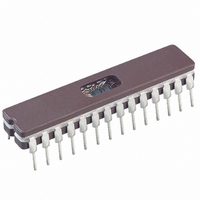
PIC18C242/JW Microchip Technology, PIC18C242/JW Datasheet - Page 22

PIC18C242/JW
Manufacturer Part Number
PIC18C242/JW
Description
IC MCU EPROM 8KX16 A/D 28CDIP
Manufacturer
Microchip Technology
Series
PIC® 18Cr
Datasheets
1.PIC16F616T-ISL.pdf
(8 pages)
2.PIC16C770-ISO.pdf
(8 pages)
3.PIC18C242-ISO.pdf
(305 pages)
4.PIC18C242-ISO.pdf
(12 pages)
Specifications of PIC18C242/JW
Core Processor
PIC
Core Size
8-Bit
Speed
40MHz
Connectivity
I²C, SPI, UART/USART
Peripherals
Brown-out Detect/Reset, LVD, POR, PWM, WDT
Number Of I /o
22
Program Memory Size
16KB (8K x 16)
Program Memory Type
EPROM, UV
Ram Size
512 x 8
Voltage - Supply (vcc/vdd)
4.2 V ~ 5.5 V
Data Converters
A/D 5x10b
Oscillator Type
External
Operating Temperature
0°C ~ 70°C
Package / Case
28-CDIP (0.300", 7.62mm) Window
Lead Free Status / RoHS Status
Contains lead / RoHS non-compliant
Eeprom Size
-
Available stocks
Company
Part Number
Manufacturer
Quantity
Price
Company:
Part Number:
PIC18C242/JW
Manufacturer:
NS
Quantity:
10
- PIC16F616T-ISL PDF datasheet
- PIC16C770-ISO PDF datasheet #2
- PIC18C242-ISO PDF datasheet #3
- PIC18C242-ISO PDF datasheet #4
- Current page: 22 of 305
- Download datasheet (6Mb)
PIC18CXX2
2.6
The PIC18CXX2 devices include a feature that allows
the system clock source to be switched from the main
oscillator to an alternate low frequency clock source.
For the PIC18CXX2 devices, this alternate clock
source is the Timer1 oscillator. If a low frequency crys-
tal (32 kHz, for example) has been attached to the
Timer1 oscillator pins and the Timer1 oscillator has
FIGURE 2-7:
2.6.1
The system clock source switching is performed under
software control. The system clock switch bit, SCS
(OSCCON<0>) controls the clock switching. When the
SCS bit is’0’, the system clock source comes from the
main oscillator that is selected by the FOSC configura-
tion bits in Configuration Register1H. When the SCS bit
is set, the system clock source will come from the
Timer1 oscillator. The SCS bit is cleared on all forms of
RESET.
REGISTER 2-1:
DS39026C-page 20
Oscillator Switching Feature
SYSTEM CLOCK SWITCH BIT
bit 7-1
bit 0
OSC2
OSC1
T1OSO
T1OSI
DEVICE CLOCK SOURCES
OSCCON REGISTER
bit 7
Unimplemented: Read as '0'
SCS: System Clock Switch bit
When OSCSEN configuration bit = ’0’ and T1OSCEN bit is set:
1 = Switch to Timer1 oscillator/clock pin
0 = Use primary oscillator/clock input pin
When OSCSEN and T1OSCEN are in other states:
bit is forced clear
Legend:
R = Readable bit
- n = Value at POR reset
U-0
—
Timer1 Oscillator
Main Oscillator
PIC18CXXX
U-0
—
SLEEP
T1OSCEN
Enable
Oscillator
U-0
W = Writable bit
’1’ = Bit is set
—
Clock Source option
for other modules
been enabled, the device can switch to a low power
execution mode. Figure 2-7 shows a block diagram of
the system clock sources. The clock switching feature
is enabled by programming the Oscillator Switching
Enable (OSCSEN) bit in Configuration Register1H to a
’0’. Clock switching is disabled in an erased device.
See Section 9.0 for further details of the Timer1 oscilla-
tor. See Section 18.0 for Configuration Register details.
4 x PLL
U-0
T
—
T
Note:
T
OSC
1
P
U = Unimplemented bit, read as ‘0’
’0’ = Bit is cleared
T
OSC
The Timer1 oscillator must be enabled and
operating to switch the system clock
source. The Timer1 oscillator is enabled by
setting the T1OSCEN bit in the Timer1
control register (T1CON). If the Timer1
oscillator is not enabled, then any write to
the SCS bit will be ignored (SCS bit forced
cleared) and the main oscillator will con-
tinue to be the system clock source.
U-0
—
/4
Source
Clock
U-0
—
2001 Microchip Technology Inc.
x = Bit is unknown
T
U-0
SCLK
—
R/W-1
SCS
bit 0
Related parts for PIC18C242/JW
Image
Part Number
Description
Manufacturer
Datasheet
Request
R

Part Number:
Description:
IC, 8BIT MCU, PIC18F, 40MHZ, LCC-44
Manufacturer:
Microchip Technology
Datasheet:

Part Number:
Description:
IC, 8BIT MCU, PIC18LF, 40MHZ, PLCC-64
Manufacturer:
Microchip Technology
Datasheet:

Part Number:
Description:
IC, 8BIT MCU, PIC18F, 64MHZ, TQFP-80
Manufacturer:
Microchip Technology
Datasheet:

Part Number:
Description:
MCU, MPU & DSP Development Tools CAN/LIN PICtail Plus Daughter Board
Manufacturer:
Microchip Technology
Datasheet:

Part Number:
Description:
IC, 8BIT MCU, PIC18F, 64MHZ, DIP-40
Manufacturer:
Microchip Technology
Datasheet:

Part Number:
Description:
IC, 8BIT MCU, PIC18LF, 40MHZ, PLCC-64
Manufacturer:
Microchip Technology
Datasheet:

Part Number:
Description:
IC, 8BIT MCU, PIC18F, 64MHZ, TQFP-64
Manufacturer:
Microchip Technology

Part Number:
Description:
IC, 8BIT MCU, PIC18F, 64MHZ, TQFP-80
Manufacturer:
Microchip Technology

Part Number:
Description:
8KB, Flash, 768bytes-RAM, 36I/O, 8-bit Family,nanowatt XLP 40 UQFN 5x5x0.5mm TUB
Manufacturer:
Microchip Technology
Datasheet:

Part Number:
Description:
8KB, Flash, 768bytes-RAM, 36I/O, 8-bit Family,nanowatt XLP 40 UQFN 5x5x0.5mm TUB
Manufacturer:
Microchip Technology

Part Number:
Description:
16KB, Flash, 768bytes-RAM, 36I/O, 8-bit Family,nanowatt XLP 40 UQFN 5x5x0.5mm TU
Manufacturer:
Microchip Technology
Datasheet:

Part Number:
Description:
16KB, Flash, 768bytes-RAM, 36I/O, 8-bit Family,nanowatt XLP 40 UQFN 5x5x0.5mm TU
Manufacturer:
Microchip Technology

Part Number:
Description:
32KB, Flash, 1536bytes-RAM, 36I/O, 8-bit Family,nanowatt XLP 40 UQFN 5x5x0.5mm T
Manufacturer:
Microchip Technology
Datasheet:

Part Number:
Description:
32KB, Flash, 1536bytes-RAM, 36I/O, 8-bit Family,nanowatt XLP 40 UQFN 5x5x0.5mm T
Manufacturer:
Microchip Technology

Part Number:
Description:
64KB, Flash, 3968bytes-RAM, 36I/O, 8-bit Family,nanowatt XLP 40 UQFN 5x5x0.5mm T
Manufacturer:
Microchip Technology
Datasheet:


