PIC18C242/JW Microchip Technology, PIC18C242/JW Datasheet - Page 207
PIC18C242/JW
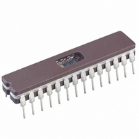
Manufacturer Part Number
PIC18C242/JW
Description
IC MCU EPROM 8KX16 A/D 28CDIP
Manufacturer
Microchip Technology
Series
PIC® 18Cr
Datasheets
1.PIC16F616T-ISL.pdf
(8 pages)
2.PIC16C770-ISO.pdf
(8 pages)
3.PIC18C242-ISO.pdf
(305 pages)
4.PIC18C242-ISO.pdf
(12 pages)
Specifications of PIC18C242/JW
Core Processor
PIC
Core Size
8-Bit
Speed
40MHz
Connectivity
I²C, SPI, UART/USART
Peripherals
Brown-out Detect/Reset, LVD, POR, PWM, WDT
Number Of I /o
22
Program Memory Size
16KB (8K x 16)
Program Memory Type
EPROM, UV
Ram Size
512 x 8
Voltage - Supply (vcc/vdd)
4.2 V ~ 5.5 V
Data Converters
A/D 5x10b
Oscillator Type
External
Operating Temperature
0°C ~ 70°C
Package / Case
28-CDIP (0.300", 7.62mm) Window
Lead Free Status / RoHS Status
Contains lead / RoHS non-compliant
Eeprom Size
-
Available stocks
Company
Part Number
Manufacturer
Quantity
Price
Company:

Part Number:
PIC18C242/JW
Manufacturer:
NS
Quantity:
10


CPFSGT
Syntax:
Operands:
Operation:
Status Affected:
Encoding:
Description:
Words:
Cycles:
Example:
Q Cycle Activity:
If skip:
If skip and followed by 2-word instruction:
2001 Microchip Technology Inc.
Before Instruction
After Instruction
operation
operation
operation
Decode
No
No
No
PC
WREG
If REG
If REG
Q1
Q1
Q1
PC
PC
register ’f’
operation
operation
operation
Compare f with WREG,
skip if f > WREG
[ label ] CPFSGT
0
a
(f)
skip if (f) > (WREG)
(unsigned comparison)
None
Compares the contents of data
memory location ’f’ to the contents
of the WREG by performing an
unsigned subtraction.
If the contents of ’f’ are greater than
the contents of WREG
fetched instruction is discarded and
a NOP is executed instead, making
this a two-cycle instruction. If ‘a’ is
0, the Access Bank will be
selected, overriding the BSR value.
If ‘a’ = 1, then the bank will be
selected as per the BSR value
(default).
1
1(2)
Note: 3 cycles if skip and followed
HERE
NGREATER
GREATER
Read
0110
No
No
No
Q2
Q2
Q2
=
=
>
=
f
[0,1]
=
WREG),
255
by a 2-word instruction.
Address (HERE)
?
WREG;
Address (GREATER)
WREG;
Address (NGREATER)
010a
operation
operation
operation
CPFSGT REG, 0
:
:
Process
Data
No
No
No
Q3
Q3
Q3
ffff
f [,a]
,
then the
operation
operation
operation
operation
No
No
No
No
Q4
Q4
Q4
ffff
CPFSLT
Syntax:
Operands:
Operation:
Status Affected:
Encoding:
Description:
Words:
Cycles:
Example:
Q Cycle Activity:
If skip:
If skip and followed by 2-word instruction:
Before Instruction
After Instruction
operation
operation
operation
Decode
PC
W
If REG
PC
If REG
PC
No
No
No
Q1
Q1
Q1
register ’f’
operation
operation
operation
Compare f with WREG,
skip if f < WREG
[ label ] CPFSLT
0
a
(f) – WREG),
skip if (f) < (WREG)
(unsigned comparison)
None
Compares the contents of data
memory location 'f' to the contents
of WREG by performing an
unsigned subtraction.
If the contents of 'f' are less than
the contents of WREG, then the
fetched instruction is discarded and
a NOP is executed instead, making
this a two-cycle instruction. If ‘a’ is
0, the Access Bank will be
selected. If ’a’ is 1, the BSR will not
be overridden (default).
1
1(2)
Note: 3 cycles if skip and followed
HERE
NLESS
LESS
Read
0110
No
No
No
Q2
Q2
Q2
=
=
<
=
f
[0,1]
=
PIC18CXX2
255
by a 2-word instruction.
Address (HERE)
?
WREG;
Address (LESS)
WREG;
Address (NLESS)
CPFSLT REG, 1
:
:
000a
operation
operation
operation
Process
Data
No
No
No
Q3
Q3
Q3
DS39026C-page 205
ffff
f [,a]
operation
operation
operation
operation
No
No
No
No
Q4
Q4
Q4
ffff
Related parts for PIC18C242/JW
Image
Part Number
Description
Manufacturer
Datasheet
Request
R

Part Number:
Description:
IC, 8BIT MCU, PIC18F, 40MHZ, LCC-44
Manufacturer:
Microchip Technology
Datasheet:
Part Number:
Description:
IC, 8BIT MCU, PIC18LF, 40MHZ, PLCC-64
Manufacturer:
Microchip Technology
Datasheet:
Part Number:
Description:
IC, 8BIT MCU, PIC18F, 64MHZ, TQFP-80
Manufacturer:
Microchip Technology
Datasheet:

Part Number:
Description:
MCU, MPU & DSP Development Tools CAN/LIN PICtail Plus Daughter Board
Manufacturer:
Microchip Technology
Datasheet:

Part Number:
Description:
IC, 8BIT MCU, PIC18F, 64MHZ, DIP-40
Manufacturer:
Microchip Technology
Datasheet:

Part Number:
Description:
IC, 8BIT MCU, PIC18LF, 40MHZ, PLCC-64
Manufacturer:
Microchip Technology
Datasheet:
Part Number:
Description:
IC, 8BIT MCU, PIC18F, 64MHZ, TQFP-64
Manufacturer:
Microchip Technology
Part Number:
Description:
IC, 8BIT MCU, PIC18F, 64MHZ, TQFP-80
Manufacturer:
Microchip Technology

Part Number:
Description:
8KB, Flash, 768bytes-RAM, 36I/O, 8-bit Family,nanowatt XLP 40 UQFN 5x5x0.5mm TUB
Manufacturer:
Microchip Technology
Datasheet:
Part Number:
Description:
8KB, Flash, 768bytes-RAM, 36I/O, 8-bit Family,nanowatt XLP 40 UQFN 5x5x0.5mm TUB
Manufacturer:
Microchip Technology
Part Number:
Description:
16KB, Flash, 768bytes-RAM, 36I/O, 8-bit Family,nanowatt XLP 40 UQFN 5x5x0.5mm TU
Manufacturer:
Microchip Technology
Datasheet:
Part Number:
Description:
16KB, Flash, 768bytes-RAM, 36I/O, 8-bit Family,nanowatt XLP 40 UQFN 5x5x0.5mm TU
Manufacturer:
Microchip Technology
Part Number:
Description:
32KB, Flash, 1536bytes-RAM, 36I/O, 8-bit Family,nanowatt XLP 40 UQFN 5x5x0.5mm T
Manufacturer:
Microchip Technology
Datasheet:
Part Number:
Description:
32KB, Flash, 1536bytes-RAM, 36I/O, 8-bit Family,nanowatt XLP 40 UQFN 5x5x0.5mm T
Manufacturer:
Microchip Technology
Part Number:
Description:
64KB, Flash, 3968bytes-RAM, 36I/O, 8-bit Family,nanowatt XLP 40 UQFN 5x5x0.5mm T
Manufacturer:
Microchip Technology
Datasheet: