PIC18C242/JW Microchip Technology, PIC18C242/JW Datasheet - Page 177
PIC18C242/JW
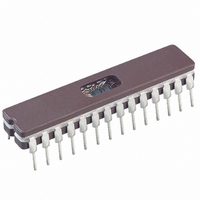
Manufacturer Part Number
PIC18C242/JW
Description
IC MCU EPROM 8KX16 A/D 28CDIP
Manufacturer
Microchip Technology
Series
PIC® 18Cr
Datasheets
1.PIC16F616T-ISL.pdf
(8 pages)
2.PIC16C770-ISO.pdf
(8 pages)
3.PIC18C242-ISO.pdf
(305 pages)
4.PIC18C242-ISO.pdf
(12 pages)
Specifications of PIC18C242/JW
Core Processor
PIC
Core Size
8-Bit
Speed
40MHz
Connectivity
I²C, SPI, UART/USART
Peripherals
Brown-out Detect/Reset, LVD, POR, PWM, WDT
Number Of I /o
22
Program Memory Size
16KB (8K x 16)
Program Memory Type
EPROM, UV
Ram Size
512 x 8
Voltage - Supply (vcc/vdd)
4.2 V ~ 5.5 V
Data Converters
A/D 5x10b
Oscillator Type
External
Operating Temperature
0°C ~ 70°C
Package / Case
28-CDIP (0.300", 7.62mm) Window
Lead Free Status / RoHS Status
Contains lead / RoHS non-compliant
Eeprom Size
-
Available stocks
Company
Part Number
Manufacturer
Quantity
Price
Company:

Part Number:
PIC18C242/JW
Manufacturer:
NS
Quantity:
10


17.1
The Low Voltage Detect Control register controls the
operation of the Low Voltage Detect circuitry.
REGISTER 17-1:
2000 Microchip Technology Inc.
Control Register
bit 7-6
bit 5
bit 4
bit 3-0
LVDCON REGISTER
bit 7
Unimplemented: Read as '0'
IRVST: Internal Reference Voltage Stable Flag bit
1 = Indicates that the Low Voltage Detect logic will generate the interrupt flag at the
0 = Indicates that the Low Voltage Detect logic will not generate the interrupt flag at the
LVDEN: Low Voltage Detect Power Enable bit
1 = Enables LVD, powers up LVD circuit
0 = Disables LVD, powers down LVD circuit
LVDL3:LVDL0: Low Voltage Detection Limit bits
1111 = External analog input is used (input comes from the LVDIN pin)
1110 = 4.5V min. - 4.77V max.
1101 = 4.2V min. - 4.45V max.
1100 = 4.0V min. - 4.24V max.
1011 = 3.8V min. - 4.03V max.
1010 = 3.6V min. - 3.82V max.
1001 = 3.5V min. - 3.71V max.
1000 = 3.3V min. - 3.50V max.
0111 = 3.0V min. - 3.18V max.
0110 = 2.8V min. - 2.97V max.
0101 = 2.7V min. - 2.86V max.
0100 = 2.5V min. - 2.65V max.
0011 = 2.4V min. - 2.54V max.
0010 = 2.2V min. - 2.33V max.
0001 = 2.0V min. - 2.12V max.
0000 = 1.8V min. - 1.91V max.
Note:
Legend:
R = Readable bit
U = Unimplemented bit, read as ‘0’
U-0
—
specified voltage range
specified voltage range and the LVD interrupt should not be enabled
LVDL3:LVDL0 modes which result in a trip point below the valid operating voltage
of the device are not tested.
U-0
—
IRVST
R-0
LVDEN
R/W-0
W = Writable bit
- n = Value at POR reset
LVDL3
R/W-0
LVDL2
R/W-1
PIC18CXX2
LVDL1
R/W-0
DS39026C-page 175
LVDL0
R/W-1
bit 0
Related parts for PIC18C242/JW
Image
Part Number
Description
Manufacturer
Datasheet
Request
R

Part Number:
Description:
IC, 8BIT MCU, PIC18F, 40MHZ, LCC-44
Manufacturer:
Microchip Technology
Datasheet:
Part Number:
Description:
IC, 8BIT MCU, PIC18LF, 40MHZ, PLCC-64
Manufacturer:
Microchip Technology
Datasheet:
Part Number:
Description:
IC, 8BIT MCU, PIC18F, 64MHZ, TQFP-80
Manufacturer:
Microchip Technology
Datasheet:

Part Number:
Description:
MCU, MPU & DSP Development Tools CAN/LIN PICtail Plus Daughter Board
Manufacturer:
Microchip Technology
Datasheet:

Part Number:
Description:
IC, 8BIT MCU, PIC18F, 64MHZ, DIP-40
Manufacturer:
Microchip Technology
Datasheet:

Part Number:
Description:
IC, 8BIT MCU, PIC18LF, 40MHZ, PLCC-64
Manufacturer:
Microchip Technology
Datasheet:
Part Number:
Description:
IC, 8BIT MCU, PIC18F, 64MHZ, TQFP-64
Manufacturer:
Microchip Technology
Part Number:
Description:
IC, 8BIT MCU, PIC18F, 64MHZ, TQFP-80
Manufacturer:
Microchip Technology

Part Number:
Description:
8KB, Flash, 768bytes-RAM, 36I/O, 8-bit Family,nanowatt XLP 40 UQFN 5x5x0.5mm TUB
Manufacturer:
Microchip Technology
Datasheet:
Part Number:
Description:
8KB, Flash, 768bytes-RAM, 36I/O, 8-bit Family,nanowatt XLP 40 UQFN 5x5x0.5mm TUB
Manufacturer:
Microchip Technology
Part Number:
Description:
16KB, Flash, 768bytes-RAM, 36I/O, 8-bit Family,nanowatt XLP 40 UQFN 5x5x0.5mm TU
Manufacturer:
Microchip Technology
Datasheet:
Part Number:
Description:
16KB, Flash, 768bytes-RAM, 36I/O, 8-bit Family,nanowatt XLP 40 UQFN 5x5x0.5mm TU
Manufacturer:
Microchip Technology
Part Number:
Description:
32KB, Flash, 1536bytes-RAM, 36I/O, 8-bit Family,nanowatt XLP 40 UQFN 5x5x0.5mm T
Manufacturer:
Microchip Technology
Datasheet:
Part Number:
Description:
32KB, Flash, 1536bytes-RAM, 36I/O, 8-bit Family,nanowatt XLP 40 UQFN 5x5x0.5mm T
Manufacturer:
Microchip Technology
Part Number:
Description:
64KB, Flash, 3968bytes-RAM, 36I/O, 8-bit Family,nanowatt XLP 40 UQFN 5x5x0.5mm T
Manufacturer:
Microchip Technology
Datasheet: