M30290FAHP#U5A Renesas Electronics America, M30290FAHP#U5A Datasheet - Page 84
M30290FAHP#U5A
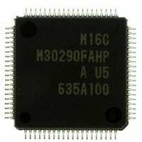
Manufacturer Part Number
M30290FAHP#U5A
Description
IC M16C/29 MCU FLASH 96K 80LQFP
Manufacturer
Renesas Electronics America
Series
M16C™ M16C/Tiny/29r
Datasheet
1.M30291FCHPU5A.pdf
(501 pages)
Specifications of M30290FAHP#U5A
Core Processor
M16C/60
Core Size
16-Bit
Speed
20MHz
Connectivity
CAN, I²C, IEBus, SIO, UART/USART
Peripherals
DMA, POR, PWM, Voltage Detect, WDT
Number Of I /o
71
Program Memory Size
96KB (96K x 8)
Program Memory Type
FLASH
Ram Size
8K x 8
Voltage - Supply (vcc/vdd)
2.7 V ~ 5.5 V
Data Converters
A/D 27x10b
Oscillator Type
Internal
Operating Temperature
-20°C ~ 85°C
Package / Case
80-LQFP
For Use With
R0K330290S000BE - KIT EVAL STARTER FOR M16C/29M30290T2-CPE - EMULATOR COMPACT M16C/26A/28/29M30290T2-CPE-HP - EMULATOR COMPACT FOR M16C/TINY
Lead Free Status / RoHS Status
Lead free / RoHS Compliant
Eeprom Size
-
Available stocks
Company
Part Number
Manufacturer
Quantity
Price

Part Number:
M30290FAHP#U5AM30290FAHP#D3
Manufacturer:
Renesas Electronics America
Quantity:
10 000
Part Number:
M30290FAHP#U5AM30290FAHP#U3A
Manufacturer:
Renesas Electronics America
Quantity:
135
Part Number:
M30290FAHP#U5AM30290FAHP#U3A
Manufacturer:
Renesas Electronics America
Quantity:
10 000


R
R
M
7.5 CPU Clock and Peripheral Function Clock
e
E
1
. v
J
Table 7.3 The function of the CLK
6
0
The CPU clock is used to operate the CPU and peripheral function clocks are used to operate the peripheral
functions.
7.5.1 CPU Clock
7.5.2 Peripheral Function Clock(f
7.5.3 ClockOutput Function
1
9
C
1 .
B
PCLK5
This is the operating clock for the CPU and watchdog timer.
The clock source for the CPU clock can be chosen to be the main clock, sub clock, on-chip oscillator clock
or the PLL clock.
If the main clock or on-chip oscillator clock is selected as the clock source for the CPU clock, the selected
clock source can be divided by 1 (undivided), 2, 4, 8 or 16 to produce the CPU clock. Use the CM06 bit in
CM0 register and bits CM17 to CM16 in CM1 register to select the divide-by-n value.
When the PLL clock is selected as the clock source for the CPU clock, the CM06 bit should be set to 0 and
bits CM17 and CM16 to 00
After reset, the on-chip oscillator clock divided by 16 provides the CPU clock.
Note that when entering stop mode from high or middle speed mode, on-chip oscillator mode or on-chip
oscillator low power dissipation mode, or when the CM05 bit in the CM0 register is set to 1 (main clock
turned off) in low-speed mode, the CM06 bit in the CM0 register is set to 1 (divide-by-8 mode).
These are operating clocks for the peripheral functions.
Of these, fi (i = 1, 2, 8, 32) and fi
divided by i. The clock fi is used for Timer A, Timer B, SI/O3 and SI/O4 while fiSIO is used for UART0 to
UART2. Additionally, the f1 and f2 clocks are also used for dead time timer, Timer S, multi-master I
The f
D converter.
The f
vided), 2, 4, 8, or 16, and is used for the CAN module.
When the WAIT instruction is executed after setting the CM02 bit in the CM0 register to 1 (peripheral
function clock turned off during wait mode), or when the MCU is in low power dissipation mode, the fi, fi
f
The f
when the sub clock is on.
Note 1: f
The f
and bits CM01 to CM00 in the CM0 register to select. Table 7.3 shows the function of the CLK
2 /
AD
0
2
9
1
0
0
0
0
1
1
1
1
M
, and f
0
G
1
r a
AD
C32
CAN0
1
0 -
o r
, f
3 .
1
u
clock is produced from the main clock, PLL clock or on-chip oscillator clock, and is used for the A/
8
, 0
1
clock is produced from the sub clock, and is used for timers A and B. This clock can only be used
CAN0
p
, f
CAN0
2
2
clock is derived from the main clock, PLL clock or on-chip oscillator clock devided by 1 (undi-
32
0
0
CM01
or f
7
clock stops at "H" in CAN0 sleep mode.
clocks are turned off. (Note 1)
0
0
1
1
0
0
1
1
C
clock can be output from the CLK
page 58
CM00
2
f o
(undivided).
0
1
0
1
0
1
0
1
4
5
SIO
8
OUT
are derived from the main clock, PLL clock, or on-chip oscillator clock
The function of the CLK
I/O port P9
f
f
f
f
Do not set
Do not set
Do not set
C
8
32
1
pin
1
, f
2
, f
0
8
, f
32
OUT
, f
1SIO
pin. Use the PCLK5 bit in the PCLKR register
OUT
, f
2SIO
pin
, f
8SIO
, f
32SIO
, f
AD
, f
C32
OUT
2
, f
C bus.
CAN0
pin.
SIO
,
)
Related parts for M30290FAHP#U5A
Image
Part Number
Description
Manufacturer
Datasheet
Request
R

Part Number:
Description:
KIT STARTER FOR M16C/29
Manufacturer:
Renesas Electronics America
Datasheet:

Part Number:
Description:
KIT STARTER FOR R8C/2D
Manufacturer:
Renesas Electronics America
Datasheet:

Part Number:
Description:
R0K33062P STARTER KIT
Manufacturer:
Renesas Electronics America
Datasheet:

Part Number:
Description:
KIT STARTER FOR R8C/23 E8A
Manufacturer:
Renesas Electronics America
Datasheet:

Part Number:
Description:
KIT STARTER FOR R8C/25
Manufacturer:
Renesas Electronics America
Datasheet:

Part Number:
Description:
KIT STARTER H8S2456 SHARPE DSPLY
Manufacturer:
Renesas Electronics America
Datasheet:

Part Number:
Description:
KIT STARTER FOR R8C38C
Manufacturer:
Renesas Electronics America
Datasheet:

Part Number:
Description:
KIT STARTER FOR R8C35C
Manufacturer:
Renesas Electronics America
Datasheet:

Part Number:
Description:
KIT STARTER FOR R8CL3AC+LCD APPS
Manufacturer:
Renesas Electronics America
Datasheet:
Part Number:
Description:
KIT STARTER FOR RX610
Manufacturer:
Renesas Electronics America
Datasheet:

Part Number:
Description:
KIT STARTER FOR R32C/118
Manufacturer:
Renesas Electronics America
Datasheet:

Part Number:
Description:
KIT DEV RSK-R8C/26-29
Manufacturer:
Renesas Electronics America
Datasheet:

Part Number:
Description:
KIT STARTER FOR SH7124
Manufacturer:
Renesas Electronics America
Datasheet:

Part Number:
Description:
KIT STARTER FOR H8SX/1622
Manufacturer:
Renesas Electronics America
Datasheet:

Part Number:
Description:
KIT DEV FOR SH7203
Manufacturer:
Renesas Electronics America
Datasheet: