M30290FAHP#U5A Renesas Electronics America, M30290FAHP#U5A Datasheet - Page 339
M30290FAHP#U5A
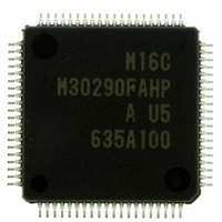
Manufacturer Part Number
M30290FAHP#U5A
Description
IC M16C/29 MCU FLASH 96K 80LQFP
Manufacturer
Renesas Electronics America
Series
M16C™ M16C/Tiny/29r
Datasheet
1.M30291FCHPU5A.pdf
(501 pages)
Specifications of M30290FAHP#U5A
Core Processor
M16C/60
Core Size
16-Bit
Speed
20MHz
Connectivity
CAN, I²C, IEBus, SIO, UART/USART
Peripherals
DMA, POR, PWM, Voltage Detect, WDT
Number Of I /o
71
Program Memory Size
96KB (96K x 8)
Program Memory Type
FLASH
Ram Size
8K x 8
Voltage - Supply (vcc/vdd)
2.7 V ~ 5.5 V
Data Converters
A/D 27x10b
Oscillator Type
Internal
Operating Temperature
-20°C ~ 85°C
Package / Case
80-LQFP
For Use With
R0K330290S000BE - KIT EVAL STARTER FOR M16C/29M30290T2-CPE - EMULATOR COMPACT M16C/26A/28/29M30290T2-CPE-HP - EMULATOR COMPACT FOR M16C/TINY
Lead Free Status / RoHS Status
Lead free / RoHS Compliant
Eeprom Size
-
Available stocks
Company
Part Number
Manufacturer
Quantity
Price

Part Number:
M30290FAHP#U5AM30290FAHP#D3
Manufacturer:
Renesas Electronics America
Quantity:
10 000
Part Number:
M30290FAHP#U5AM30290FAHP#U3A
Manufacturer:
Renesas Electronics America
Quantity:
135
Part Number:
M30290FAHP#U5AM30290FAHP#U3A
Manufacturer:
Renesas Electronics America
Quantity:
10 000


R
R
M
18. CRC Calculation Circuit
18.1 CRC Snoop
e
E
1
. v
J
Figure 18.1 CRC circuit block diagram
6
0
The Cyclic Redundancy Check (CRC) calculation detects errors in blocks of data. The MCU uses a gen-
erator polynomial of CRC_CCITT (X
code.
The CRC code is a 16-bit code generated for a block of a given data length in multiples of bytes. The code
is updated in the CRC data register everytime one byte of data is transferred to a CRC input register. The
data register must be initialized before use. Generation of CRC code for one byte of data is completed in
two machine cycles.
Figure 18.1 shows the block diagram of the CRC circuit. Figure 18.2 shows the CRC-related registers.
Figure 18.3 shows the calculation example using the CRC_CCITT operation.
The CRC circuit includes the ability to snoop reads and writes to certain SFR addresses. This can be used
to accumulate the CRC value on a stream of data without using extra bandwidth to explicitly write data into
the CRCIN register. All SFR addresses after 0020
useful to snoop the writes to a UART TX buffer, or the reads from a UART RX buffer.
To snoop an SFR address, the target address is written to the CRC snoop Address Register (CRCSAR).
The two most significant bits of this register enable snooping on reads or writes to the target address. If the
target SFR is written to by the CPU or DMA, and the CRC snoop write bit is set (CRCSW=1), the CRC will
latch the data into the CRCIN register. The new CRC code will be set in the CRCD register.
Similarly, if the target SFR is read by the CRC or DMA, and the CRC snoop read bit is set (CRCSR=1), the
CRC will latch the data from the target into the CRCIN register and calculate the CRC.
The CRC circuit can only calculate CRC codes on data byte at a time. Therefore, if a target SFR is
accessed in word (16 bit), only one low-order byte data is stored into the CRCIN register.
1
9
C
1 .
B
2 /
0
2
9
1
M
0
G
1
r a
0 -
o r
3 .
1
u
, 0
1
p
2
2
0
0
7
CRC input register (8)
page 313
x
16
+ x
CRC code generating circuit
12
Data bus high-order
Eight low-order bits
Address Bus
Data bus low-order
+ x
CRCD register (16)
5
f o
+ 1 OR x
4
5
8
(Address 03BE
16
+ X
16
+ x
12
15
+ x
+ X
16
2
)
+ 1
5
Eight high-order bits
+ 1) or CRC-16 (X
16
are subject to the CRC snoop. The CRC snoop is
(Address 03BD
16
, 03BC
16
16
+ X
)
15
Snoop Address
+ X
Equal?
2
+ 1) to generate CRC
enable
Snoop
SnoopB
lock
Related parts for M30290FAHP#U5A
Image
Part Number
Description
Manufacturer
Datasheet
Request
R

Part Number:
Description:
KIT STARTER FOR M16C/29
Manufacturer:
Renesas Electronics America
Datasheet:

Part Number:
Description:
KIT STARTER FOR R8C/2D
Manufacturer:
Renesas Electronics America
Datasheet:

Part Number:
Description:
R0K33062P STARTER KIT
Manufacturer:
Renesas Electronics America
Datasheet:

Part Number:
Description:
KIT STARTER FOR R8C/23 E8A
Manufacturer:
Renesas Electronics America
Datasheet:

Part Number:
Description:
KIT STARTER FOR R8C/25
Manufacturer:
Renesas Electronics America
Datasheet:

Part Number:
Description:
KIT STARTER H8S2456 SHARPE DSPLY
Manufacturer:
Renesas Electronics America
Datasheet:

Part Number:
Description:
KIT STARTER FOR R8C38C
Manufacturer:
Renesas Electronics America
Datasheet:

Part Number:
Description:
KIT STARTER FOR R8C35C
Manufacturer:
Renesas Electronics America
Datasheet:

Part Number:
Description:
KIT STARTER FOR R8CL3AC+LCD APPS
Manufacturer:
Renesas Electronics America
Datasheet:
Part Number:
Description:
KIT STARTER FOR RX610
Manufacturer:
Renesas Electronics America
Datasheet:

Part Number:
Description:
KIT STARTER FOR R32C/118
Manufacturer:
Renesas Electronics America
Datasheet:

Part Number:
Description:
KIT DEV RSK-R8C/26-29
Manufacturer:
Renesas Electronics America
Datasheet:

Part Number:
Description:
KIT STARTER FOR SH7124
Manufacturer:
Renesas Electronics America
Datasheet:

Part Number:
Description:
KIT STARTER FOR H8SX/1622
Manufacturer:
Renesas Electronics America
Datasheet:

Part Number:
Description:
KIT DEV FOR SH7203
Manufacturer:
Renesas Electronics America
Datasheet: