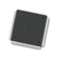
MCF5208CAB166 Freescale Semiconductor, MCF5208CAB166 Datasheet - Page 43

MCF5208CAB166
Manufacturer Part Number
MCF5208CAB166
Description
MCU 32BIT 166.67MHZ 160-QFP
Manufacturer
Freescale Semiconductor
Series
MCF520xr
Datasheet
1.MCF5207CVM166J.pdf
(46 pages)
Specifications of MCF5208CAB166
Core Processor
Coldfire V2
Core Size
32-Bit
Speed
166.67MHz
Connectivity
EBI/EMI, Ethernet, I²C, SPI, UART/USART
Peripherals
DMA, WDT
Number Of I /o
50
Program Memory Type
ROMless
Ram Size
16K x 8
Voltage - Supply (vcc/vdd)
1.4 V ~ 3.6 V
Oscillator Type
External
Operating Temperature
-40°C ~ 85°C
Package / Case
160-QFP
Family Name
MCF5xxx
Device Core
ColdFire
Device Core Size
32b
Frequency (max)
166.67MHz
Instruction Set Architecture
RISC
Supply Voltage 1 (typ)
1.8/2.5/3.3V
Operating Supply Voltage (max)
1.6/1.95/2.75/3.6V
Operating Supply Voltage (min)
1.4/1.7/2.25/3V
Operating Temp Range
-40C to 85C
Operating Temperature Classification
Industrial
Mounting
Surface Mount
Pin Count
160
Package Type
PQFP
Processor Series
MCF520x
Core
ColdFire V2
3rd Party Development Tools
JLINK-CF-BDM26, EWCF
Lead Free Status / RoHS Status
Lead free / RoHS Compliant
Eeprom Size
-
Program Memory Size
-
Data Converters
-
Lead Free Status / Rohs Status
Compliant
Available stocks
Company
Part Number
Manufacturer
Quantity
Price
Company:
Part Number:
MCF5208CAB166
Manufacturer:
SANREX
Quantity:
210
Company:
Part Number:
MCF5208CAB166
Manufacturer:
Freescale Semiconductor
Quantity:
10 000
6
Freescale Semiconductor
Revision
Number
Revision History
0.1
0.2
0.3
0
5/23/2005
6/16/2005
8/26/2005
9/07/2005
Date
MCF5208 ColdFire
Cleaned up various electrical specifications:
• Initial Release
• Corrected 144QFP pinout in
• Changed maximum core frequency in
• Changed ball M9 from SD_VDD to EVDD in
•
•
•
•
• Added filtering circuits and voltage sequencing sections:
• Removed “Operating Conditions” table from
•
• Corrected DRAMSEL footnote #3 in
• Updated
• Added 144MAPBGA ballmap to
• Changed J12 from PLL_VDD to IVDD in
Table 26. Revision History
FEC functionality, which are actually UART 0/1 clear-to-send and
request-to-send signals.
166.67MHz. Also, changed symbols in table: f
for consistency throughout document and reference manual.
Table
SD_VDD. BE/BWE[3:0] for 144 LQFP should be “20, 48, 18, 50“ instead
of “18, 20, 48, 50”
Table
synthesizer supply voltage” to “PLL supply voltage”, changed min PLLV
from -0.5 to -0.3, changed max V
from -65 to -55,
Table
Table
maximum from 1.65 to 1.6, added PLL supply voltage entry, added pad
supply entries for mobile-DDR, DDR, and SDR, changed minimum input
high voltage from 0.7xEV
changed minimum input low voltage from VSS-0.3 to -0.05 and maximum
from 0.35xEV
mobile-DDR, removed high impedance leakage current entry, changed
minimum output high voltage from EV
output high/low voltage entries, removed load capacitance and DC
injection current entries.
“PLL Power Filtering,”
Separation Cautions.”
PLL Electrical Characteristics,”
Table
reference and on-chip PLL frequency specs to have only a CLKOUT
frequency spec of TBD to 83.33MHz, removed loss of reference frequency
and self-clocked mode frequency entries, in EXTAL input high/low voltage
entries changed “All other modes (Dual controller (1:1), Bypass, External)”
to “All other modes (External, Limp)”, removed XTAL output high/low
voltage entries, removed power-up to lock time entry, removed last 5
entries (frequency un-lock range, frequency lock range, CLKOUT period
jitter, frequency modulation range limit, and ICO frequency)
®
3: Pin 33 for 144 LQFP package should be EVDD instead of
4: Added DDR/Memory pad supply voltage spec, changed “clock
5: Changed TBD values in T
7: Changed minimum core supply voltage from 1.35 to 1.4 and
11: Changed minimum core frequency to TBD, removed external
Microprocessor Data Sheet, Rev. 3
Table 3
DD
to 0.8, added input high/low voltage entries for DDR and
with 144MAPBGA pin locations.
and
Substantive Changes
DD
Section 5.4.2, “Supply Voltage Sequencing and
to 2 and maximum from 3.65 to EV
Figure
because it is redundant with
IN
Section 4.3, “Pinout—144 MAPBGA.”
j
from 4.0 to 3.6, changed minimum T
entry to 105°C.
1. Pins 139-142 incorrectly showed
Table
DD
Table
-0.5 to EV
Figure
3.
10, spec #2, from 240MHz to
Section 5.6, “Oscillator and
Figure
core
9.
DD
-> f
9.
-0.4, added DDR/bus
sys
and f
Section 5.4.1,
Revision History
Table
sys
DD
-> f
+0.05,
7.
sys/2
DD
stg
43


