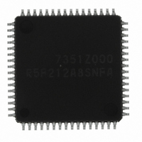
R5F212A8SNFA#U0 Renesas Electronics America, R5F212A8SNFA#U0 Datasheet - Page 515

R5F212A8SNFA#U0
Manufacturer Part Number
R5F212A8SNFA#U0
Description
IC R8C/2A MCU FLASH 64K 64-LQFP
Manufacturer
Renesas Electronics America
Series
R8C/2x/2Ar
Specifications of R5F212A8SNFA#U0
Core Processor
R8C
Core Size
16/32-Bit
Speed
20MHz
Connectivity
I²C, LIN, SIO, SSU, UART/USART
Peripherals
POR, PWM, Voltage Detect, WDT
Number Of I /o
55
Program Memory Size
64KB (64K x 8)
Program Memory Type
FLASH
Ram Size
3K x 8
Voltage - Supply (vcc/vdd)
2.2 V ~ 5.5 V
Data Converters
A/D 12x10b; D/A 2x8b
Oscillator Type
Internal
Operating Temperature
-20°C ~ 85°C
Package / Case
64-LQFP
For Use With
R0K5212D8S001BE - KIT STARTER FOR R8C/2DR0K5212D8S000BE - KIT DEV FOR R8C/2D
Lead Free Status / RoHS Status
Lead free / RoHS Compliant
Eeprom Size
-
Available stocks
Company
Part Number
Manufacturer
Quantity
Price
Part Number:
R5F212A8SNFA#U0R5F212A8SNFA#V2
Manufacturer:
Renesas Electronics America
Quantity:
10 000
- Current page: 515 of 611
- Download datasheet (7Mb)
R8C/2A Group, R8C/2B Group
Rev.2.00
REJ09B0324-0200
Figure 20.4
20.3.2
Option Function Select Register
b7 b6 b5 b4 b3 b2 b1 b0
NOTES:
1.
2.
3. If the block including the OFS register is erased, FFh is set to the OFS register.
1
The ROM code protect function disables reading or changing the contents of the on-chip flash memory by the
OFS register in parallel I/O mode. Figure 20.4 shows the OFS Register.
The ROM code protect function is enabled by writing 0 to the ROMCP1 bit and 1 to the ROMCR bit. It disables
reading or changing the contents of the on-chip flash memory.
Once ROM code protect is enabled, the content in the internal flash memory cannot be rewritten in parallel I/O
mode. To disable ROM code protect, erase the block including the OFS register with CPU rewrite mode or
standard serial I/O mode.
The OFS register is on the flash memory. Write to the OFS register w ith a program. After w riting is completed, do not
w rite additions to the OFS register.
To use the pow er-on reset, set the LVD0ON bit to 0 (voltage monitor 0 reset enabled after hardw are reset).
Nov 26, 2007
1
ROM Code Protect Function
OFS Register
1
Bit Symbol
CSPROINI
ROMCP1
LVD0ON
WDTON
ROMCR
Symbol
OFS
(b1)
(b4)
(b6)
Page 493 of 580
—
—
—
Watchdog timer start
select bit
Reserved bit
ROM code protect
disabled bit
ROM code protect bit
Reserved bit
Voltage detection 0
circuit start bit
Reserved bit
Count source protect
mode after reset select
bit
(1)
Address
Bit Name
0FFFFh
(2)
0 : Starts w atchdog timer automatically after reset
1 : Watchdog timer is inactive after reset
Set to 1.
0 : ROM code protect disabled
1 : ROMCP1 enabled
0 : ROM code protect enabled
1 : ROM code protect disabled
Set to 1.
0 : Voltage monitor 0 reset enabled after hardw are
1 : Voltage monitor 0 reset disabled after hardw are
Set to 1.
0 : Count source protect mode enabled after reset
1 : Count source protect mode disabled after reset
reset
reset
When Shipping
Function
FFh
(3)
20. Flash Memory
RW
RW
RW
RW
RW
RW
RW
RW
RW
Related parts for R5F212A8SNFA#U0
Image
Part Number
Description
Manufacturer
Datasheet
Request
R

Part Number:
Description:
KIT STARTER FOR M16C/29
Manufacturer:
Renesas Electronics America
Datasheet:

Part Number:
Description:
KIT STARTER FOR R8C/2D
Manufacturer:
Renesas Electronics America
Datasheet:

Part Number:
Description:
R0K33062P STARTER KIT
Manufacturer:
Renesas Electronics America
Datasheet:

Part Number:
Description:
KIT STARTER FOR R8C/23 E8A
Manufacturer:
Renesas Electronics America
Datasheet:

Part Number:
Description:
KIT STARTER FOR R8C/25
Manufacturer:
Renesas Electronics America
Datasheet:

Part Number:
Description:
KIT STARTER H8S2456 SHARPE DSPLY
Manufacturer:
Renesas Electronics America
Datasheet:

Part Number:
Description:
KIT STARTER FOR R8C38C
Manufacturer:
Renesas Electronics America
Datasheet:

Part Number:
Description:
KIT STARTER FOR R8C35C
Manufacturer:
Renesas Electronics America
Datasheet:

Part Number:
Description:
KIT STARTER FOR R8CL3AC+LCD APPS
Manufacturer:
Renesas Electronics America
Datasheet:

Part Number:
Description:
KIT STARTER FOR RX610
Manufacturer:
Renesas Electronics America
Datasheet:

Part Number:
Description:
KIT STARTER FOR R32C/118
Manufacturer:
Renesas Electronics America
Datasheet:

Part Number:
Description:
KIT DEV RSK-R8C/26-29
Manufacturer:
Renesas Electronics America
Datasheet:

Part Number:
Description:
KIT STARTER FOR SH7124
Manufacturer:
Renesas Electronics America
Datasheet:

Part Number:
Description:
KIT STARTER FOR H8SX/1622
Manufacturer:
Renesas Electronics America
Datasheet:

Part Number:
Description:
KIT DEV FOR SH7203
Manufacturer:
Renesas Electronics America
Datasheet:


