MC56F8011VFAE Freescale Semiconductor, MC56F8011VFAE Datasheet - Page 23
MC56F8011VFAE
Manufacturer Part Number
MC56F8011VFAE
Description
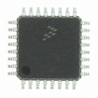
IC DIGITAL SIGNAL CTLR 32-LQFP
Manufacturer
Freescale Semiconductor
Series
56F8xxxr
Datasheet
1.MC56F8013VFAE.pdf
(126 pages)
Specifications of MC56F8011VFAE
Core Processor
56800
Core Size
16-Bit
Speed
32MHz
Connectivity
I²C, SCI, SPI
Peripherals
POR, PWM, WDT
Number Of I /o
26
Program Memory Size
12KB (6K x 16)
Program Memory Type
FLASH
Ram Size
1K x 16
Voltage - Supply (vcc/vdd)
3 V ~ 3.6 V
Data Converters
A/D 6x12b
Oscillator Type
Internal
Operating Temperature
-40°C ~ 105°C
Package / Case
32-LQFP
Product
DSCs
Data Bus Width
16 bit
Processor Series
MC56F80xx
Core
56800E
Numeric And Arithmetic Format
Fixed-Point
Device Million Instructions Per Second
32 MIPs
Maximum Clock Frequency
32 MHz
Number Of Programmable I/os
26
Data Ram Size
2 KB
Operating Supply Voltage
3.3 V
Maximum Operating Temperature
+ 105 C
Mounting Style
SMD/SMT
Development Tools By Supplier
MC56F8037EVM, DEMO56F8014-EE, DEMO56F8013-EE
Interface Type
SCI, SPI, I2C
Minimum Operating Temperature
- 40 C
For Use With
CPA56F8013 - BOARD SOCKET FOR MC56F8013APMOTOR56F8000E - KIT DEMO MOTOR CTRL SYSTEM
Lead Free Status / RoHS Status
Lead free / RoHS Compliant
Eeprom Size
-
Lead Free Status / Rohs Status
Lead free / RoHS Compliant
Available stocks
Company
Part Number
Manufacturer
Quantity
Price
Company:

Part Number:
MC56F8011VFAE
Manufacturer:
Freescale
Quantity:
1
Company:
Part Number:
MC56F8011VFAE
Manufacturer:
Freescale Semiconductor
Quantity:
10 000


Freescale Semiconductor
Table 2-3 56F8013/56F8011 Signal and Package Information for the 32-Pin LQFP (Continued)
7. This signal is also brought out on the GPIOB2 pin.
Return to
(FAULT1)
GPIOA1
GPIOA2
GPIOA3
GPIOA4
(PWM1)
(PWM2)
(PWM3)
(PWM4)
Signal
Name
(T2
7
)
Table 2-2
Pin No.
LQFP
28
23
24
22
Output
Output
Output
Output
Output
Output
Output
Output
Output
Input/
Input/
Input/
Input/
Input/
Type
Input
State During
Input with
Input with
Input with
Input with
enabled
enabled
enabled
enabled
internal
internal
internal
internal
56F8013/56F8011 Data Sheet, Rev. 12
pull-up
pull-up
pull-up
pull-up
Reset
Port A GPIO — This GPIO pin can be individually programmed as
an input or output pin.
PWM1 — This is one of the six PWM output pins.
After reset, the default state is GPIOA1.
Port A GPIO — This GPIO pin can be individually programmed as
an input or output pin.
PWM2 — This is one of the six PWM output pins.
After reset, the default state is GPIOA2.
Port A GPIO — This GPIO pin can be individually programmed as
an input or output pin.
PWM3 — This is one of the six PWM output pins.
After reset, the default state is GPIOA3.
Port A GPIO — This GPIO pin can be individually programmed as
an input or output pin.
PWM4 — This is one of the six PWM output pins.
Fault1 — This fault input pin is used for disabling selected PWM
outputs in cases where fault conditions originate off-chip.
T2 — Timer, Channel 2
After reset, the default state is GPIOA4. The alternative peripheral
functionality is controlled via the SIM. See
Signal Description
Section
56F8013/56F8011 Signal Pins
6.3.8.
23
Related parts for MC56F8011VFAE
Image
Part Number
Description
Manufacturer
Datasheet
Request
R

Part Number:
Description:
16-bit Digital Signal Controllers
Manufacturer:
Freescale Semiconductor, Inc
Datasheet:
Part Number:
Description:
Manufacturer:
Freescale Semiconductor, Inc
Datasheet:
Part Number:
Description:
Manufacturer:
Freescale Semiconductor, Inc
Datasheet:
Part Number:
Description:
Manufacturer:
Freescale Semiconductor, Inc
Datasheet:
Part Number:
Description:
Manufacturer:
Freescale Semiconductor, Inc
Datasheet:
Part Number:
Description:
Manufacturer:
Freescale Semiconductor, Inc
Datasheet:
Part Number:
Description:
Manufacturer:
Freescale Semiconductor, Inc
Datasheet:
Part Number:
Description:
Manufacturer:
Freescale Semiconductor, Inc
Datasheet:
Part Number:
Description:
Manufacturer:
Freescale Semiconductor, Inc
Datasheet:
Part Number:
Description:
Manufacturer:
Freescale Semiconductor, Inc
Datasheet:
Part Number:
Description:
Manufacturer:
Freescale Semiconductor, Inc
Datasheet:
Part Number:
Description:
Manufacturer:
Freescale Semiconductor, Inc
Datasheet:
Part Number:
Description:
Manufacturer:
Freescale Semiconductor, Inc
Datasheet:
Part Number:
Description:
Manufacturer:
Freescale Semiconductor, Inc
Datasheet:
Part Number:
Description:
Manufacturer:
Freescale Semiconductor, Inc
Datasheet: