MC56F8011VFAE Freescale Semiconductor, MC56F8011VFAE Datasheet - Page 19
MC56F8011VFAE
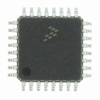
Manufacturer Part Number
MC56F8011VFAE
Description
IC DIGITAL SIGNAL CTLR 32-LQFP
Manufacturer
Freescale Semiconductor
Series
56F8xxxr
Datasheet
1.MC56F8013VFAE.pdf
(126 pages)
Specifications of MC56F8011VFAE
Core Processor
56800
Core Size
16-Bit
Speed
32MHz
Connectivity
I²C, SCI, SPI
Peripherals
POR, PWM, WDT
Number Of I /o
26
Program Memory Size
12KB (6K x 16)
Program Memory Type
FLASH
Ram Size
1K x 16
Voltage - Supply (vcc/vdd)
3 V ~ 3.6 V
Data Converters
A/D 6x12b
Oscillator Type
Internal
Operating Temperature
-40°C ~ 105°C
Package / Case
32-LQFP
Product
DSCs
Data Bus Width
16 bit
Processor Series
MC56F80xx
Core
56800E
Numeric And Arithmetic Format
Fixed-Point
Device Million Instructions Per Second
32 MIPs
Maximum Clock Frequency
32 MHz
Number Of Programmable I/os
26
Data Ram Size
2 KB
Operating Supply Voltage
3.3 V
Maximum Operating Temperature
+ 105 C
Mounting Style
SMD/SMT
Development Tools By Supplier
MC56F8037EVM, DEMO56F8014-EE, DEMO56F8013-EE
Interface Type
SCI, SPI, I2C
Minimum Operating Temperature
- 40 C
For Use With
CPA56F8013 - BOARD SOCKET FOR MC56F8013APMOTOR56F8000E - KIT DEMO MOTOR CTRL SYSTEM
Lead Free Status / RoHS Status
Lead free / RoHS Compliant
Eeprom Size
-
Lead Free Status / Rohs Status
Lead free / RoHS Compliant
Available stocks
Company
Part Number
Manufacturer
Quantity
Price
Company:

Part Number:
MC56F8011VFAE
Manufacturer:
Freescale
Quantity:
1
Company:
Part Number:
MC56F8011VFAE
Manufacturer:
Freescale Semiconductor
Quantity:
10 000


Freescale Semiconductor
Table 2-3 56F8013/56F8011 Signal and Package Information for the 32-Pin LQFP (Continued)
2. This signal is also brought out on the GPIOB0 pin.
Return to
(GPIOA7)
GPIOB7
GPIOB4
(CLKO)
RESET
(SCL
Signal
Name
(TXD)
(T0)
2
)
Table 2-2
Pin No.
LQFP
15
19
3
Input/Open
Output
Output
Output
Output
Output
Output
Output
Input/
Input/
Input/
Input/
Type
Drain
Input
State During
Input with
Input with
Input with
enabled
enabled
enabled
internal
internal
internal
56F8013/56F8011 Data Sheet, Rev. 12
pull-up
pull-up
pull-up
Reset
Port B GPIO — This GPIO pin can be individually programmed as
an input or output pin.
Transmit Data — SCI transmit data output or transmit / receive in
single wire operation.
Serial Clock — This pin serves as the I
After reset, the default state is GPIOB7. The alternative peripheral
functionality is controlled via the SIM. See
Reset — This input is a direct hardware reset on the processor.
When RESET is asserted low, the chip is initialized and placed in the
reset state. A Schmitt trigger input is used for noise immunity. The
internal reset signal will be deasserted synchronous with the internal
clocks after a fixed number of internal clocks.
Port A GPIO — This GPIO pin can be individually programmed as
an input or open drain output pin. Note that RESET functionality is
disabled in this mode and the chip can only be reset via POR, COP
reset, or software reset.
After reset, the default state is RESET.
Port B GPIO — This GPIO pin can be individually programmed as
an input or output pin.
T0 — Timer, Channel 0
Clock Output — This is a buffered clock signal. Using the
SIM_CLKO Select Register (SIM_CLKOSR), this pin can be
programmed as any of the following: disabled (logic 0), CLK_MSTR
(system clock), IPBus clock, or oscillator output. See
After reset, the default state is GPIOB4. The alternative peripheral
functionality is controlled via the SIM. See
Signal Description
2
C serial clock.
Section
Section
56F8013/56F8011 Signal Pins
6.3.8.
6.3.8.
Section
6.3.7.
19
Related parts for MC56F8011VFAE
Image
Part Number
Description
Manufacturer
Datasheet
Request
R

Part Number:
Description:
16-bit Digital Signal Controllers
Manufacturer:
Freescale Semiconductor, Inc
Datasheet:
Part Number:
Description:
Manufacturer:
Freescale Semiconductor, Inc
Datasheet:
Part Number:
Description:
Manufacturer:
Freescale Semiconductor, Inc
Datasheet:
Part Number:
Description:
Manufacturer:
Freescale Semiconductor, Inc
Datasheet:
Part Number:
Description:
Manufacturer:
Freescale Semiconductor, Inc
Datasheet:
Part Number:
Description:
Manufacturer:
Freescale Semiconductor, Inc
Datasheet:
Part Number:
Description:
Manufacturer:
Freescale Semiconductor, Inc
Datasheet:
Part Number:
Description:
Manufacturer:
Freescale Semiconductor, Inc
Datasheet:
Part Number:
Description:
Manufacturer:
Freescale Semiconductor, Inc
Datasheet:
Part Number:
Description:
Manufacturer:
Freescale Semiconductor, Inc
Datasheet:
Part Number:
Description:
Manufacturer:
Freescale Semiconductor, Inc
Datasheet:
Part Number:
Description:
Manufacturer:
Freescale Semiconductor, Inc
Datasheet:
Part Number:
Description:
Manufacturer:
Freescale Semiconductor, Inc
Datasheet:
Part Number:
Description:
Manufacturer:
Freescale Semiconductor, Inc
Datasheet:
Part Number:
Description:
Manufacturer:
Freescale Semiconductor, Inc
Datasheet: