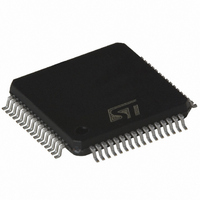
ST72F521AR9TC STMicroelectronics, ST72F521AR9TC Datasheet - Page 202

ST72F521AR9TC
Manufacturer Part Number
ST72F521AR9TC
Description
IC MCU 8BIT 60K FLASH 64-TQFP
Manufacturer
STMicroelectronics
Series
ST7r
Datasheet
1.ST72F521M9T6.pdf
(215 pages)
Specifications of ST72F521AR9TC
Core Processor
ST7
Core Size
8-Bit
Speed
8MHz
Connectivity
CAN, I²C, SCI, SPI
Peripherals
LVD, POR, PWM, WDT
Number Of I /o
48
Program Memory Size
60KB (60K x 8)
Program Memory Type
FLASH
Ram Size
2K x 8
Voltage - Supply (vcc/vdd)
3.8 V ~ 5.5 V
Data Converters
A/D 16x10b
Oscillator Type
Internal
Operating Temperature
-40°C ~ 125°C
Package / Case
64-TQFP, 64-VQFP
For Use With
497-6453 - BOARD EVAL BASED ON ST7LNBX
Lead Free Status / RoHS Status
Lead free / RoHS Compliant
Eeprom Size
-
Available stocks
Company
Part Number
Manufacturer
Quantity
Price
Company:
Part Number:
ST72F521AR9TC
Manufacturer:
STMicroelectronics
Quantity:
10 000
Company:
Part Number:
ST72F521AR9TCE
Manufacturer:
STMicroelectronics
Quantity:
10 000
Company:
Part Number:
ST72F521AR9TCTR
Manufacturer:
STMicroelectronics
Quantity:
10 000
ST72F521, ST72521B
ST72521 DEVICE CONFIGURATION AND ORDERING INFORMATION (Cont’d)
OPT2 = Reserved, must be kept at default value.
OPT1= PKG0 Package selection bit 0
This option bit is used to select the package (see
table in PKG1 option bit description).
OPT0= FMP_R Flash memory read-out protection
Read-out protection, when selected, provides a
protection against Program Memory content ex-
traction and against write access to Flash memo-
ry.
Erasing the option bytes when the FMP_R option
is selected causes the whole user memory to be
erased first, and the device can be reprogrammed.
Refer to
gramming Reference Manual for more details.
Note: Readout protection is not supported if LVD
is enabled.
0: Read-out protection enabled
1: Read-out protection disabled
OPTION BYTE 1
OPT7= PKG1 Package selection bit 1
This option bit, with the PKG0 bit, selects the pack-
age.
Note: On the chip, each I/O port has 8 pads. Pads
that are not bonded to external pins are in input
pull-up configuration after reset. The configuration
of these pads must be kept at reset state to avoid
added current consumption.
OPT6 = RSTC RESET clock cycle selection
This option bit selects the number of CPU cycles
applied during the RESET phase and when exiting
HALT mode. For resonator oscillators, it is advised
to select 4096 due to the long crystal stabilization
time.
0: Reset phase with 4096 CPU cycles
1: Reset phase with 256 CPU cycles
202/215
Version
(A)R
M
Section 4.3.1
Selected Package
TQFP80
TQFP64
and the ST7 Flash Pro-
PKG 1 PKG 0
1
1
1
0
OPT5:4 = OSCTYPE[1:0] Oscillator Type
These option bits select the ST7 main clock
source type.
OPT3:1 = OSCRANGE[2:0] Oscillator range
When the resonator oscillator type is selected,
these option bits select the resonator oscillator
current source corresponding to the frequency
range of the used resonator. Otherwise, these bits
are used to select the normal operating frequency
range.
OPT0 = PLLOFF PLL activation
This option bit activates the PLL which allows mul-
tiplication by two of the main input clock frequency.
The PLL must not be used with the internal RC os-
cillator or with external clock source. The PLL is
guaranteed only with an input frequency between
2 and 4MHz.
0: PLL x2 enabled
1: PLL x2 disabled
CAUTION: the PLL can be enabled only if the
“OSC RANGE” (OPT3:1) bits are configured to
“MP - 2~4MHz”. Otherwise, the device functionali-
ty is not guaranteed.
Resonator Oscillator
Reserved
Internal RC Oscillator
External Source
LP
MP
MS
HS
Typ. Freq. Range
Clock Source
8~16MHz
1~2MHz
2~4MHz
4~8MHz
2
0
0
0
0
OSCRANGE
1
0
0
1
1
OSCTYPE
1
0
0
1
1
0
0
1
0
1
0
0
1
0
1


