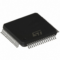
ST72F521AR9TC STMicroelectronics, ST72F521AR9TC Datasheet - Page 113

ST72F521AR9TC
Manufacturer Part Number
ST72F521AR9TC
Description
IC MCU 8BIT 60K FLASH 64-TQFP
Manufacturer
STMicroelectronics
Series
ST7r
Datasheet
1.ST72F521M9T6.pdf
(215 pages)
Specifications of ST72F521AR9TC
Core Processor
ST7
Core Size
8-Bit
Speed
8MHz
Connectivity
CAN, I²C, SCI, SPI
Peripherals
LVD, POR, PWM, WDT
Number Of I /o
48
Program Memory Size
60KB (60K x 8)
Program Memory Type
FLASH
Ram Size
2K x 8
Voltage - Supply (vcc/vdd)
3.8 V ~ 5.5 V
Data Converters
A/D 16x10b
Oscillator Type
Internal
Operating Temperature
-40°C ~ 125°C
Package / Case
64-TQFP, 64-VQFP
For Use With
497-6453 - BOARD EVAL BASED ON ST7LNBX
Lead Free Status / RoHS Status
Lead free / RoHS Compliant
Eeprom Size
-
Available stocks
Company
Part Number
Manufacturer
Quantity
Price
Company:
Part Number:
ST72F521AR9TC
Manufacturer:
STMicroelectronics
Quantity:
10 000
Company:
Part Number:
ST72F521AR9TCE
Manufacturer:
STMicroelectronics
Quantity:
10 000
Company:
Part Number:
ST72F521AR9TCTR
Manufacturer:
STMicroelectronics
Quantity:
10 000
- Current page: 113 of 215
- Download datasheet (5Mb)
SERIAL COMMUNICATIONS INTERFACE (Cont’d)
DATA REGISTER (SCIDR)
Read/Write
Reset Value: Undefined
Contains the Received or Transmitted data char-
acter, depending on whether it is read from or writ-
ten to.
The Data register performs a double function (read
and write) since it is composed of two registers,
one for transmission (TDR) and one for reception
(RDR).
The TDR register provides the parallel interface
between the internal bus and the output shift reg-
ister (see
The RDR register provides the parallel interface
between the input shift register and the internal
bus (see
BAUD RATE REGISTER (SCIBRR)
Read/Write
Reset Value: 0000 0000 (00h)
Bits 7:6= SCP[1:0] First SCI Prescaler
These 2 prescaling bits allow several standard
clock division ranges:
SCP1
DR7
7
7
PR Prescaling factor
SCP0
DR6
Figure
Figure
13
SCT2
1
3
4
DR5
60).
60).
SCT1
DR4
SCT0
DR3
SCP1
SCR2 SCR1 SCR0
DR2
0
0
1
1
DR1
SCP0
0
1
0
1
DR0
0
0
Bits 5:3 = SCT[2:0] SCI Transmitter rate divisor
These 3 bits, in conjunction with the SCP1 & SCP0
bits define the total division applied to the bus
clock to yield the transmit rate clock in convention-
al Baud Rate Generator mode.
Bits 2:0 = SCR[2:0] SCI Receiver rate divisor.
These 3 bits, in conjunction with the SCP[1:0] bits
define the total division applied to the bus clock to
yield the receive rate clock in conventional Baud
Rate Generator mode.
RR Dividing factor
TR dividing factor
128
128
16
32
64
16
32
64
1
2
4
8
1
2
4
8
SCR2
SCT2
ST72F521, ST72521B
0
0
0
0
1
1
1
1
0
0
0
0
1
1
1
1
SCR1
SCT1
0
0
1
1
0
0
1
1
0
0
1
1
0
0
1
1
SCR0
113/215
SCT0
0
1
0
1
0
1
0
1
0
1
0
1
0
1
0
1
Related parts for ST72F521AR9TC
Image
Part Number
Description
Manufacturer
Datasheet
Request
R

Part Number:
Description:
80/64-PIN 8-BIT MCU WITH 32 TO 60K FLASH/ROM ADC FIVE TIMERS SPI SCI I2C CAN INTERFACE
Manufacturer:
STMicroelectronics

Part Number:
Description:
STMicroelectronics [RIPPLE-CARRY BINARY COUNTER/DIVIDERS]
Manufacturer:
STMicroelectronics
Datasheet:

Part Number:
Description:
STMicroelectronics [LIQUID-CRYSTAL DISPLAY DRIVERS]
Manufacturer:
STMicroelectronics
Datasheet:

Part Number:
Description:
BOARD EVAL FOR MEMS SENSORS
Manufacturer:
STMicroelectronics
Datasheet:

Part Number:
Description:
NPN TRANSISTOR POWER MODULE
Manufacturer:
STMicroelectronics
Datasheet:

Part Number:
Description:
TURBOSWITCH ULTRA-FAST HIGH VOLTAGE DIODE
Manufacturer:
STMicroelectronics
Datasheet:

Part Number:
Description:
Manufacturer:
STMicroelectronics
Datasheet:

Part Number:
Description:
DIODE / SCR MODULE
Manufacturer:
STMicroelectronics
Datasheet:

Part Number:
Description:
DIODE / SCR MODULE
Manufacturer:
STMicroelectronics
Datasheet:

Part Number:
Description:
Search -----> STE16N100
Manufacturer:
STMicroelectronics
Datasheet:

Part Number:
Description:
Search ---> STE53NA50
Manufacturer:
STMicroelectronics
Datasheet:

Part Number:
Description:
NPN Transistor Power Module
Manufacturer:
STMicroelectronics
Datasheet:


