ST7FDALIF2M6TR STMicroelectronics, ST7FDALIF2M6TR Datasheet - Page 131

ST7FDALIF2M6TR
Manufacturer Part Number
ST7FDALIF2M6TR
Description
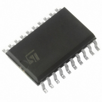
IC MCU 8BIT 8K FLASH 20-SOIC
Manufacturer
STMicroelectronics
Series
ST7r
Datasheet
1.ST7DALI-EVAL.pdf
(171 pages)
Specifications of ST7FDALIF2M6TR
Core Processor
ST7
Core Size
8-Bit
Speed
8MHz
Connectivity
DALI, SPI
Peripherals
LVD, POR, PWM, WDT
Number Of I /o
15
Program Memory Size
8KB (8K x 8)
Program Memory Type
FLASH
Eeprom Size
256 x 8
Ram Size
384 x 8
Voltage - Supply (vcc/vdd)
2.4 V ~ 5.5 V
Data Converters
A/D 7x10b
Oscillator Type
Internal
Operating Temperature
-40°C ~ 85°C
Package / Case
20-SOIC (7.5mm Width)
Processor Series
ST7DALI
Core
ST7
Data Bus Width
8 bit
Data Ram Size
384 B
Interface Type
DALI, SPI
Maximum Clock Frequency
8 MHz
Number Of Programmable I/os
15
Number Of Timers
3
Maximum Operating Temperature
+ 85 C
Mounting Style
SMD/SMT
Development Tools By Supplier
ST7FLITE-SK/RAIS, ST7DALI-EVAL, ST7MDT10-DVP3, ST7MDT10-EMU3, STX-RLINK
Minimum Operating Temperature
- 40 C
On-chip Adc
10 bit, 7 Channel / 13 bit, 7 Channel
Lead Free Status / RoHS Status
Lead free / RoHS Compliant
Available stocks
Company
Part Number
Manufacturer
Quantity
Price
Company:
Part Number:
ST7FDALIF2M6TR
Manufacturer:
NEC
Quantity:
670
ST7DALIF2
20.3.1
20.3.2
20.3.3
Operating conditions with low voltage detector (LVD)
T
Table 66.
1. Not tested in production.
2. Not tested in production. The V
3. Use of LVD with capacitive power supply: with this type of power supply, if power cuts occur in the
Auxiliary Voltage Detector (AVD) Thresholds
T
Table 67.
1.
Internal RC oscillator and PLL
The ST7 internal clock can be supplied by an internal RC oscillator and PLL (selectable by
option byte).
V
V
V
Vt
t
I
V
Symbol
Symbol
A
A
V
g(VDD)
DD(LVD
IT+
IT-
hys
IT+
IT-
ΔV
POR
V
= -40 to 85°C, unless otherwise specified
= -40 to 85°C, unless otherwise specified
and LVD reset. When the V
MCU.
application, it is recommended to pull V
example in
Not tested in production.
(LVD)
hys
(AVD)
(LVD)
(AVD)
IT-
)
Reset release threshold
(V
Reset generation threshold
(V
LVD voltage threshold
hysteresis
V
Filtered glitch delay on V
LVD/AVD current consumption
1=>0 AVDF flag toggle
threshold
(V
0=>1 AVDF flag toggle
threshold
(V
AVD voltage threshold
hysteresis
Voltage drop between AVD
flag set and LVD reset
activation
DD
DD
DD
DD
DD
Figure 87 on page 150
Power on/power down operating conditions
AVD thresholds
rise time rate
rise)
fall)
rise)
fall)
Parameter
Parameter
DD
(2)(3)
slope is outside these values, the LVD may not ensure a proper reset of the
DD
rise time rate condition is needed to insure a correct device power-on
and note 4.
DD
DD
down to 0V to ensure optimum restart conditions. Refer to circuit
High Threshold
Med. Threshold
Low Threshold
High Threshold
Med. Threshold
Low Threshold
V
Not detected by the
LVD
High Threshold
Med. Threshold
Low Threshold
High Threshold
Med. Threshold
Low Threshold
V
V
IT+
IT+
DD
(LVD)
(AVD)
fall
Conditions
Conditions
-V
-V
IT-
IT-
(LVD)
(AVD)
3.40
2.65
4.00
4.40
3.90
3.20
3.80
3.20
2.40
Min
4.30
3.70
2.90
Min
20
(1)
(1)
Electrical characteristics
(1)
(1)
(1)
(1)
4.70
4.10
3.40
4.60
3.90
3.20
0.45
4.25
3.60
2.90
4.05
3.40
2.70
Typ
150
Typ
200
220
4.30
3.65
2.90
4.90
4.10
3.40
20000
Max
4.50
3.80
3.15
Max
5.00
4.30
3.60
150
(1)
(1)
(1)
(1)
(1)
(1)
131/171
μs/V
Unit
Unit
mV
mV
μA
ns
V
V
V


