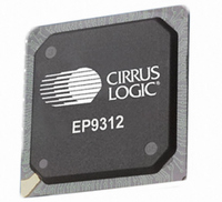
EP9312-IB Cirrus Logic Inc, EP9312-IB Datasheet - Page 613

EP9312-IB
Manufacturer Part Number
EP9312-IB
Description
IC ARM920T MCU 200MHZ 352-PBGA
Manufacturer
Cirrus Logic Inc
Series
EP9r
Datasheets
1.EP9307-CRZ.pdf
(824 pages)
2.EP9312-IBZ.pdf
(4 pages)
3.EP9312-CB.pdf
(62 pages)
4.EP9312-CB.pdf
(17 pages)
Specifications of EP9312-IB
Core Processor
ARM9
Core Size
16/32-Bit
Speed
200MHz
Connectivity
EBI/EMI, EIDE, Ethernet, I²C, IrDA, Keypad/Touchscreen, SPI, UART/USART, USB
Peripherals
AC'97, DMA, I²:S, LCD, LED, MaverickKey, POR, PWM, WDT
Number Of I /o
16
Program Memory Type
ROMless
Ram Size
32K x 8
Voltage - Supply (vcc/vdd)
1.65 V ~ 3.6 V
Data Converters
A/D 8x12b
Oscillator Type
External
Operating Temperature
-40°C ~ 85°C
Package / Case
352-BGA
Processor Series
EP93xx
Core
ARM920T
Data Bus Width
32 bit
3rd Party Development Tools
MDK-ARM, RL-ARM, ULINK2
Lead Free Status / RoHS Status
Contains lead / RoHS non-compliant
Eeprom Size
-
Program Memory Size
-
Lead Free Status / Rohs Status
No
Other names
598-1259
Available stocks
Company
Part Number
Manufacturer
Quantity
Price
Company:
Part Number:
EP9312-IBZ
Manufacturer:
CIRRUS
Quantity:
30
Company:
Part Number:
EP9312-IBZ
Manufacturer:
HITTITE
Quantity:
1 200
- EP9307-CRZ PDF datasheet
- EP9312-IBZ PDF datasheet #2
- EP9312-CB PDF datasheet #3
- EP9312-CB PDF datasheet #4
- Current page: 613 of 824
- Download datasheet (13Mb)
DS785UM1
17.5.2 Functional Description
17.5.2.1 Baud Rate Generation
signalled. The CRC computation logic is preset to all ones before reception/transmission of
each frame and the result is inverted before it used for comparison or transmission. Note that
unlike the address, control and data fields, the 32 bit inverted CRC value is transmitted and
received from least significant byte to most significant and within each byte the least
significant nibble is encoded/decoded first. The cyclical redundancy checker uses the 32
term polynomial:
CRC(x) =
Following reset, the FIR is disabled. Reset also causes the transmit and receive buffers and
tail register to be flushed (buffers marked as empty). To transmit data in FIR mode, use the
following procedure:
The baud rate is derived by dividing down a fixed 48 MHz clock. The 8 MHz baud (time-slot)
clock for the receiver is synchronized with the 4 PPM data stream each time a transition is
detected on the receive data line using a digital PLL. To encode a 4.0 Mbps data stream, the
required “symbol” frequency is 2.0 MHz, with four chips per symbol at a frequency of
8.0 MHz. Receive data is sampled half way through each time-slot period by counting three
out of the six 48 MHz clock periods which make up each chip. Refer to
page
preamble consists of four symbols repeated sixteen times. This repeating pattern is used to
identify the first time-slot or beginning of a symbol and resets the two bit chip counter logic,
such that the 4 PPM data is properly decoded.
1. Set the EN bits in the IrEnable register to 11b for FIR mode. Do not begin data
2. Before enabling the FIR, the user must first clear any writable or “sticky” status bits that
3. Next, the desired mode of operation is programmed in the control register. Set the TXE
4. Write 1 to 3 bytes to the appropriate IrDataTail register.
5. Once the FIR is enabled, transmission/reception of data can begin on the transmit and
(x
transmission.
are set by writing a one to each bit. (A sticky bit is a readable status bit that may be
cleared by writing a one to its location.) Set the TAB and TFC bits in the FISR register,
then read the FISR register to clear all interrupts.
and RXE bits in the IrCtrl register.
receive pins.
32
17-15. The symbols are synchronized during preamble reception. Recall that the
+ x
26
+ x
23
+ x
22
+ x
16
Copyright 2007 Cirrus Logic
+ x
12
+ x
11
+ x
10
+ x
8
+ x
7
+ x
5
+ x
4
+ x
2
Figure 17-3 on
+ x + 1)
EP93xx User’s Guide
17-17
IrDA
17
Related parts for EP9312-IB
Image
Part Number
Description
Manufacturer
Datasheet
Request
R

Part Number:
Description:
IC ARM920T MCU 200MHZ 352-PBGA
Manufacturer:
Cirrus Logic Inc
Datasheet:

Part Number:
Description:
IC ARM9 SOC UNIVERSAL 352PBGA
Manufacturer:
Cirrus Logic Inc
Datasheet:

Part Number:
Description:
System-on-Chip Processor
Manufacturer:
Cirrus Logic Inc
Datasheet:

Part Number:
Description:
IC ARM920T MCU 200MHZ 352-PBGA
Manufacturer:
Cirrus Logic Inc
Datasheet:

Part Number:
Description:
IC ARM920T MCU 200MHZ 352-PBGA
Manufacturer:
Cirrus Logic Inc
Datasheet:

Part Number:
Description:
IC ARM920T MCU 166MHZ 208-LQFP
Manufacturer:
Cirrus Logic Inc
Datasheet:

Part Number:
Description:
IC ARM920T MCU 166MHZ 208-LQFP
Manufacturer:
Cirrus Logic Inc
Datasheet:

Part Number:
Description:
Development Kit
Manufacturer:
Cirrus Logic Inc
Datasheet:

Part Number:
Description:
Development Kit
Manufacturer:
Cirrus Logic Inc
Datasheet:

Part Number:
Description:
High-efficiency PFC + Fluorescent Lamp Driver Reference Design
Manufacturer:
Cirrus Logic Inc
Datasheet:

Part Number:
Description:
Development Kit
Manufacturer:
Cirrus Logic Inc
Datasheet:

Part Number:
Description:
Development Kit
Manufacturer:
Cirrus Logic Inc
Datasheet:

Part Number:
Description:
Ref Bd For Speakerbar MSA & DSP Products
Manufacturer:
Cirrus Logic Inc


