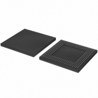
LPC3180FEL320/01,5 NXP Semiconductors, LPC3180FEL320/01,5 Datasheet - Page 48

LPC3180FEL320/01,5
Manufacturer Part Number
LPC3180FEL320/01,5
Description
IC ARM9 MCU 208MHZ 320-LFBGA
Manufacturer
NXP Semiconductors
Series
LPC3000r
Specifications of LPC3180FEL320/01,5
Package / Case
320-LFBGA
Core Processor
ARM9
Core Size
16/32-Bit
Speed
208MHz
Connectivity
EBI/EMI, I²C, MMC, SPI, UART/USART, USB OTG
Peripherals
DMA, PWM, WDT
Number Of I /o
55
Program Memory Type
ROMless
Ram Size
64K x 8
Voltage - Supply (vcc/vdd)
1.1 V ~ 3.3 V
Data Converters
A/D 3x10b
Oscillator Type
External
Operating Temperature
-40°C ~ 85°C
Processor Series
LPC31
Core
ARM926EJ-S
Data Bus Width
32 bit
Maximum Clock Frequency
208 MHz
Operating Supply Voltage
1.8 V / 3V
Maximum Operating Temperature
+ 85 C
Mounting Style
SMD/SMT
3rd Party Development Tools
MDK-ARM, RL-ARM, ULINK2
Development Tools By Supplier
OM10096
Minimum Operating Temperature
- 40 C
Package
320LFBGA
Device Core
ARM926EJ-S
Family Name
LPC3100
Maximum Speed
208 MHz
Number Of Programmable I/os
55
Interface Type
I2C/SPI/UART/USB
On-chip Adc
3-chx10-bit
Number Of Timers
2
Lead Free Status / RoHS Status
Lead free / RoHS Compliant
For Use With
622-1018 - EVAL KIT FOR LP3180568-4063 - KIT DEV LPC3180568-4062 - DEBUGGER J-LINK JTAG568-4061 - DEBUGGER U-LINK2 JTAG FOR NXP
Eeprom Size
-
Program Memory Size
-
Lead Free Status / Rohs Status
Lead free / RoHS Compliant
Other names
568-4529
935286983551
935286983551
Available stocks
Company
Part Number
Manufacturer
Quantity
Price
Company:
Part Number:
LPC3180FEL320/01,5
Manufacturer:
NXP Semiconductors
Quantity:
10 000
NXP Semiconductors
11. Appendix
LPC3180_01_1
Preliminary data sheet
11.1 Compatibility with LPC3180
This appendix provides compatibility and comparison information between the LPC3180
and the LPC3180/01.
1. The reset states on 2 pins of each SPI have changed to better fit typical uses of this
2. The USB block has been integrated into the AHB Matrix. There are small USB timing
3. The pull-ups and pull-downs on the JTAG pins have been changed in order to comply
4. Pull-ups are removed from the following pins on UART7:
5. The LPC3180 I
6. Many power, ground, and internally connected pins on the LPC3180 are different from
7. LPC3180/01 U3_TX and U3_RX pads connect to the VDD_IOD power rail instead of
type of interface.
– On reset, the LPC3180 configures the SPI1_CLK and SPI1_DATIO pins as outputs
– On reset, the LPC3180 configures the SPI2_CLK and SPI2_DATIO pins as outputs
changes that result from the integration of the USB block into the AHB matrix. These
timing differences are application dependant and are unlikely to affect existing
applications. Integration of the USB block into the AHB Matrix results in the following
differences:
– The USB block gets its timing from the AHB Matrix, which means the USB_HCLK
– The USB DMA controller can now access the internal SRAM in addition to external
with IEEE JTAG recommendations. This should have no impact on compatibility.
– The pull-up on TCK is removed.
– The pull-down on NRST is changed to a pull-up.
– U7_RX
– U7_HCTS
This change should not affect backward compatibility, with the exception that if the
pins are not used they should be pulled either high or low externally.
enhanced I
master operation.
the LPC3180/01. See
compatibility.
the VDD_IOA power rail. This only affects backward compatibility on existing
LPC3180 projects that use a 1.8 V supply for domain VDD_IO1828, the input voltage
range on the U3_RX pin and the output voltage of the U3_TX pin will change from 1.8
V to 3 V.
and drives them low; In contrast, the LPC3180/01 configures these pins as inputs
and they should be pulled either high or low externally if not used.
and drives them low; In contrast, the LPC3180/01 configures these pins as inputs
and thet should be pulled either high or low externally if not used.
signal is no longer needed. As a result, the USB clock enable bit PWR_CTRL [6] is
no longer needed. This bit is reserved in the LPC3180/01. Writing to this register
bit has no effect; the value read from this register bit is undefined.
memory
2
C-bus block that supports slave and multi-master operation in addition to
2
Rev. 00.08 — 20 November 2008
C-bus supports master operation only. The LPC3180/01 has an
16/32-bit ARM microcontroller with external memory interface
Table 16
for details. This change should not affect backward
LPC3180/01
© NXP B.V. 2008. All rights reserved.
48 of 56


