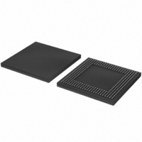
LPC3180FEL320/01,5 NXP Semiconductors, LPC3180FEL320/01,5 Datasheet - Page 34

LPC3180FEL320/01,5
Manufacturer Part Number
LPC3180FEL320/01,5
Description
IC ARM9 MCU 208MHZ 320-LFBGA
Manufacturer
NXP Semiconductors
Series
LPC3000r
Specifications of LPC3180FEL320/01,5
Package / Case
320-LFBGA
Core Processor
ARM9
Core Size
16/32-Bit
Speed
208MHz
Connectivity
EBI/EMI, I²C, MMC, SPI, UART/USART, USB OTG
Peripherals
DMA, PWM, WDT
Number Of I /o
55
Program Memory Type
ROMless
Ram Size
64K x 8
Voltage - Supply (vcc/vdd)
1.1 V ~ 3.3 V
Data Converters
A/D 3x10b
Oscillator Type
External
Operating Temperature
-40°C ~ 85°C
Processor Series
LPC31
Core
ARM926EJ-S
Data Bus Width
32 bit
Maximum Clock Frequency
208 MHz
Operating Supply Voltage
1.8 V / 3V
Maximum Operating Temperature
+ 85 C
Mounting Style
SMD/SMT
3rd Party Development Tools
MDK-ARM, RL-ARM, ULINK2
Development Tools By Supplier
OM10096
Minimum Operating Temperature
- 40 C
Package
320LFBGA
Device Core
ARM926EJ-S
Family Name
LPC3100
Maximum Speed
208 MHz
Number Of Programmable I/os
55
Interface Type
I2C/SPI/UART/USB
On-chip Adc
3-chx10-bit
Number Of Timers
2
Lead Free Status / RoHS Status
Lead free / RoHS Compliant
For Use With
622-1018 - EVAL KIT FOR LP3180568-4063 - KIT DEV LPC3180568-4062 - DEBUGGER J-LINK JTAG568-4061 - DEBUGGER U-LINK2 JTAG FOR NXP
Eeprom Size
-
Program Memory Size
-
Lead Free Status / Rohs Status
Lead free / RoHS Compliant
Other names
568-4529
935286983551
935286983551
Available stocks
Company
Part Number
Manufacturer
Quantity
Price
Company:
Part Number:
LPC3180FEL320/01,5
Manufacturer:
NXP Semiconductors
Quantity:
10 000
NXP Semiconductors
9. Dynamic characteristics
Table 7.
T
[1]
[2]
Table 8.
T
[1]
[2]
[3]
[4]
[5]
LPC3180_01_1
Preliminary data sheet
Symbol
Reset
f
External clock
f
Port pins
t
t
Symbol
f
T
t
t
t
t
t
t
t
t
t
t
t
W(RESET_N)
ext
r
f
oper
CLCX
CHCX
d(CV)
h(C)
d(AV)
h(A)
d(QV)
h(Q)
su(D)
h(D)
QZ
amb
a
CLCL
=
Parameters are valid over operating temperature range unless otherwise specified.
Supplied by an external crystal.
Parameters are valid over operating temperature range unless otherwise specified.
All values valid for EMC pads set to high slew rate. VDD_EMC = 1.8 ± 0.18 V. VDD_CORE = 1.2 ± 0.12 V or EMC pads set to low slew
rate. VDD_EMC = 3.3 ± 0.3 V. VDD_CORE = 1.2 ± 0.12 V.
f
Applies to signals: DQM, CSN, RASN, CASN, WEN, CKE.
CMD_DLY = COMMAND_DELAY bitfield in SDRAMCLK_CTRL[18:14] register.
−
oper
=
40
−
40
= 1/t
°
C to +85
°
Dynamic characteristics
EMC SDR SDRAM memory interface dynamic characteristics for LPC3180/01
Parameter
operating frequency
clock cycle time
clock LOW time
clock HIGH time
control valid delay time
control hold time
address valid delay time
address hold time
data output valid delay time
data output hold time
data input set-up time
data input hold time
data output high-impedance time
C to +85
CLCL
9.1 Clocking and I/O Port pins
9.2 SDR SDRAM controller
Parameter
external RESET_N pulse width
external clock frequency
rise time
fall time
°
C, unless otherwise specified.
°
C, unless otherwise specified.
Rev. 00.08 — 20 November 2008
[1][2]
[3]
[4]
[4]
16/32-bit ARM microcontroller with external memory interface
[1]
Conditions
Min
-
-
-
-
-
-
-
-
(CMD_DLY x 0.25) + 2.7
(CMD_DLY x 0.25) + 1.2
(CMD_DLY x 0.25) + 1.2
(CMD_DLY x 0.25) + 3.4
(CMD_DLY x 0.25) + 3.5
(CMD_DLY x 0.25) + 1.2
[2]
[2]
Min
10
1
-
-
Typical
104
9.6
4.8
4.8
0.6
0.9
Typ
-
13
5
5
LPC3180/01
<T
© NXP B.V. 2008. All rights reserved.
Max
104
CLCL
Max
-
20
-
-
-
-
-
-
-
-
-
-
34 of 56
Unit
ms
MHz
ns
ns
MHz
ns
ns
ns
ns
ns
ns
Unit
ns
ns
ns
ns
ns
ns


