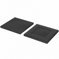
LPC3180FEL320/01,5 NXP Semiconductors, LPC3180FEL320/01,5 Datasheet - Page 26

LPC3180FEL320/01,5
Manufacturer Part Number
LPC3180FEL320/01,5
Description
IC ARM9 MCU 208MHZ 320-LFBGA
Manufacturer
NXP Semiconductors
Series
LPC3000r
Specifications of LPC3180FEL320/01,5
Package / Case
320-LFBGA
Core Processor
ARM9
Core Size
16/32-Bit
Speed
208MHz
Connectivity
EBI/EMI, I²C, MMC, SPI, UART/USART, USB OTG
Peripherals
DMA, PWM, WDT
Number Of I /o
55
Program Memory Type
ROMless
Ram Size
64K x 8
Voltage - Supply (vcc/vdd)
1.1 V ~ 3.3 V
Data Converters
A/D 3x10b
Oscillator Type
External
Operating Temperature
-40°C ~ 85°C
Processor Series
LPC31
Core
ARM926EJ-S
Data Bus Width
32 bit
Maximum Clock Frequency
208 MHz
Operating Supply Voltage
1.8 V / 3V
Maximum Operating Temperature
+ 85 C
Mounting Style
SMD/SMT
3rd Party Development Tools
MDK-ARM, RL-ARM, ULINK2
Development Tools By Supplier
OM10096
Minimum Operating Temperature
- 40 C
Package
320LFBGA
Device Core
ARM926EJ-S
Family Name
LPC3100
Maximum Speed
208 MHz
Number Of Programmable I/os
55
Interface Type
I2C/SPI/UART/USB
On-chip Adc
3-chx10-bit
Number Of Timers
2
Lead Free Status / RoHS Status
Lead free / RoHS Compliant
For Use With
622-1018 - EVAL KIT FOR LP3180568-4063 - KIT DEV LPC3180568-4062 - DEBUGGER J-LINK JTAG568-4061 - DEBUGGER U-LINK2 JTAG FOR NXP
Eeprom Size
-
Program Memory Size
-
Lead Free Status / Rohs Status
Lead free / RoHS Compliant
Other names
568-4529
935286983551
935286983551
Available stocks
Company
Part Number
Manufacturer
Quantity
Price
Company:
Part Number:
LPC3180FEL320/01,5
Manufacturer:
NXP Semiconductors
Quantity:
10 000
NXP Semiconductors
LPC3180_01_1
Preliminary data sheet
6.24.4 APB bus
6.24.5 FAB bus
6.25.1 EmbeddedICE
6.25.2 Embedded trace buffer
6.25 Emulation and debugging
Many peripheral functions are accessed by on-chip APB busses that are attached to the
higher speed AHB bus. The APB bus performs reads and writes to peripheral registers in
three peripheral clocks.
Some peripherals are placed on a special bus called FAB that allows faster CPU access
to those peripheral functions. Write access to FAB peripherals takes a single AHB clock.
Read access to FAB peripherals takes two AHB clocks.
The LPC3180/01 supports emulation and debugging via a dedicated JTAG serial port. An
Embedded Trace Buffer allows tracing program execution. The dedicated JTAG port
allows debugging of all chip features without impact to any pins that may be used in the
application.
Standard ARM EmbeddedICE logic provides on-chip debug support. The debugging of
the target system requires a host computer running the debugger software and an
EmbeddedICE protocol converter. The EmbeddedICE protocol converter converts the
Remote Debug Protocol commands to the JTAG data needed to access the ARM core.
The ARM core has a Debug Communication Channel function built-in. The debug
communication channel allows a program running on the target to communicate with the
host debugger or another separate host without stopping the program flow or entering the
debug state.
The Embedded Trace Module (ETM) is connected directly to the ARM core. It compresses
the trace information and exports it through a narrow trace port. An internal Embedded
Trace Buffer of 2 k × 24 bits captures the trace information under software debugger
control. Data from the Embedded Trace Buffer is recovered by the debug software
through the JTAG port.
The trace contains information about when the ARM core switches between states.
Instruction trace (or PC trace) shows the flow of execution of the processor and provides a
list of all the instructions that were executed. Instruction trace is significantly compressed
by only broadcasting branch addresses as well as a set of status signals that indicate the
pipeline status on a cycle by cycle basis. For data accesses either data or address or both
can be traced.
Rev. 00.08 — 20 November 2008
16/32-bit ARM microcontroller with external memory interface
LPC3180/01
© NXP B.V. 2008. All rights reserved.
26 of 56


