LPC3180FEL320/01,5 NXP Semiconductors, LPC3180FEL320/01,5 Datasheet - Page 32
LPC3180FEL320/01,5
Manufacturer Part Number
LPC3180FEL320/01,5
Description
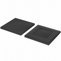
IC ARM9 MCU 208MHZ 320-LFBGA
Manufacturer
NXP Semiconductors
Series
LPC3000r
Specifications of LPC3180FEL320/01,5
Package / Case
320-LFBGA
Core Processor
ARM9
Core Size
16/32-Bit
Speed
208MHz
Connectivity
EBI/EMI, I²C, MMC, SPI, UART/USART, USB OTG
Peripherals
DMA, PWM, WDT
Number Of I /o
55
Program Memory Type
ROMless
Ram Size
64K x 8
Voltage - Supply (vcc/vdd)
1.1 V ~ 3.3 V
Data Converters
A/D 3x10b
Oscillator Type
External
Operating Temperature
-40°C ~ 85°C
Processor Series
LPC31
Core
ARM926EJ-S
Data Bus Width
32 bit
Maximum Clock Frequency
208 MHz
Operating Supply Voltage
1.8 V / 3V
Maximum Operating Temperature
+ 85 C
Mounting Style
SMD/SMT
3rd Party Development Tools
MDK-ARM, RL-ARM, ULINK2
Development Tools By Supplier
OM10096
Minimum Operating Temperature
- 40 C
Package
320LFBGA
Device Core
ARM926EJ-S
Family Name
LPC3100
Maximum Speed
208 MHz
Number Of Programmable I/os
55
Interface Type
I2C/SPI/UART/USB
On-chip Adc
3-chx10-bit
Number Of Timers
2
Lead Free Status / RoHS Status
Lead free / RoHS Compliant
For Use With
622-1018 - EVAL KIT FOR LP3180568-4063 - KIT DEV LPC3180568-4062 - DEBUGGER J-LINK JTAG568-4061 - DEBUGGER U-LINK2 JTAG FOR NXP
Eeprom Size
-
Program Memory Size
-
Lead Free Status / Rohs Status
Lead free / RoHS Compliant
Other names
568-4529
935286983551
935286983551
Available stocks
Company
Part Number
Manufacturer
Quantity
Price
Company:

Part Number:
LPC3180FEL320/01,5
Manufacturer:
NXP Semiconductors
Quantity:
10 000


NXP Semiconductors
[2]
[3]
[4]
[5]
[6]
[7]
[8]
[9]
[10] 3-state outputs go into 3-state mode when V
[11] Accounts for 100 mV voltage drop in all supply lines.
[12] Only allowed for a short time period.
Table 6.
V
[1]
[2]
[3]
[4]
[5]
[6]
[7]
LPC3180_01_1
Preliminary data sheet
Symbol
V
C
E
E
E
E
E
R
DDA
IA
ia
D
L(adj)
O
G
T
vsi
Applies to VDD_CORE12_01 to VDD_CORE12_08 pins.
Applies to pins VDD_RTC12, VDD_RTCCORE12, and VDD_RTCOSC12.
Applies to pins VDD_COREFXD12_01 to VDD_COREFXD12_02, VDD_OSC12, VDD_PLL397_12, VDD_PLLHCLK_12,
VDD_PLLUSB_12, and VDD12.
Applies to VDD_RAM, VDD_IOC pins.
Applies to VDD_IOA, VDD_IOB, and VDD_IOD pins.
Referenced to the applicable V
Including voltage on outputs in 3-state mode.
The applicable V
Conditions: V
The ADC is monotonic, there are no missing codes.
The differential linearity error (E
The integral non-linearity (E
appropriate adjustment of gain and offset errors. See
The offset error (E
ideal curve. See
The gain error (E
error, and the straight line which fits the ideal transfer curve. See
The absolute error (E
ADC and the ideal transfer curve. See
= 3.3 V; T
ADC static characteristics
Parameter
analog input voltage
analog input capacitance
differential linearity error
integral non-linearity
offset error
gain error
absolute error
voltage source interface resistance
amb
8.1.1 Power Supply Sequencing
SSA
8.2 Analog to digital Converter (ADC) static characteristics
DD
= 25
Figure
G
= 0 V, V
O
) is the relative difference in percent between the straight line fitting the actual transfer curve after removing offset
) is the absolute difference between the straight line which fits the actual curve and the straight line which fits the
voltage for the pin must be present.
T
°
) is the maximum difference between the center of the steps of the actual transfer curve of the non-calibrated
C unless otherwise specified; ADC frequency 4.5 MHz.
The LPC32x0 has no power sequencing requirements, that is, VDD(1V2), VDD(SDRAM),
VDD(IO), and VDDA(3V0) can be switched ‘On’ or ‘Off’ independent of each other. An
internal circuit takes care that the system correctly powers up in the absence of
core-power. During IO power-up this circuit takes care the system is powered in a defined
mode, and during core power-down the same is valid.
5.
DDA
L(adj)
= 3.3 V.
DD
D
) is the peak difference between the center of the steps of the actual and the ideal transfer curve after
) is the difference between the actual step width and the ideal step width. See
for the pin.
Figure
DD(3V0)
5.
Rev. 00.08 — 20 November 2008
is grounded.
16/32-bit ARM microcontroller with external memory interface
Figure
Conditions
5.
Figure
5.
[1][2][3]
[1][4]
[1][5]
[1][6]
[1][7]
Min
0
-
-
-
-
-
-
-
Typ
-
-
±0.5
±0.6
±1
±0.3
-
LPC3180/01
Max
V
1
±1
±1
±3
±0.6
±4
40
Figure
DDA
© NXP B.V. 2008. All rights reserved.
5.
Unit
V
pF
LSB
LSB
LSB
%
LSB
kΩ
32 of 56
Related parts for LPC3180FEL320/01,5
Image
Part Number
Description
Manufacturer
Datasheet
Request
R

Part Number:
Description:
NXP Semiconductors designed the LPC2420/2460 microcontroller around a 16-bit/32-bitARM7TDMI-S CPU core with real-time debug interfaces that include both JTAG andembedded trace
Manufacturer:
NXP Semiconductors
Datasheet:

Part Number:
Description:
NXP Semiconductors designed the LPC2458 microcontroller around a 16-bit/32-bitARM7TDMI-S CPU core with real-time debug interfaces that include both JTAG andembedded trace
Manufacturer:
NXP Semiconductors
Datasheet:
Part Number:
Description:
NXP Semiconductors designed the LPC2468 microcontroller around a 16-bit/32-bitARM7TDMI-S CPU core with real-time debug interfaces that include both JTAG andembedded trace
Manufacturer:
NXP Semiconductors
Datasheet:
Part Number:
Description:
NXP Semiconductors designed the LPC2470 microcontroller, powered by theARM7TDMI-S core, to be a highly integrated microcontroller for a wide range ofapplications that require advanced communications and high quality graphic displays
Manufacturer:
NXP Semiconductors
Datasheet:
Part Number:
Description:
NXP Semiconductors designed the LPC2478 microcontroller, powered by theARM7TDMI-S core, to be a highly integrated microcontroller for a wide range ofapplications that require advanced communications and high quality graphic displays
Manufacturer:
NXP Semiconductors
Datasheet:
Part Number:
Description:
The Philips Semiconductors XA (eXtended Architecture) family of 16-bit single-chip microcontrollers is powerful enough to easily handle the requirements of high performance embedded applications, yet inexpensive enough to compete in the market for hi
Manufacturer:
NXP Semiconductors
Datasheet:
Part Number:
Description:
The XA-S3 device is a member of Philips Semiconductors? XA(eXtended Architecture) family of high performance 16-bitsingle-chip microcontrollers
Manufacturer:
NXP Semiconductors
Datasheet:

Part Number:
Description:
The NXP BlueStreak LH75401/LH75411 family consists of two low-cost 16/32-bit System-on-Chip (SoC) devices
Manufacturer:
NXP Semiconductors
Datasheet:
Part Number:
Description:
The NXP LPC3130/3131 combine an 180 MHz ARM926EJ-S CPU core, high-speed USB2
Manufacturer:
NXP Semiconductors
Datasheet:
Part Number:
Description:
The NXP LPC3141 combine a 270 MHz ARM926EJ-S CPU core, High-speed USB 2
Manufacturer:
NXP Semiconductors
Part Number:
Description:
The NXP LPC3143 combine a 270 MHz ARM926EJ-S CPU core, High-speed USB 2
Manufacturer:
NXP Semiconductors

Part Number:
Description:
The NXP LPC3152 combines an 180 MHz ARM926EJ-S CPU core, High-speed USB 2
Manufacturer:
NXP Semiconductors
Part Number:
Description:
The NXP LPC3154 combines an 180 MHz ARM926EJ-S CPU core, High-speed USB 2
Manufacturer:
NXP Semiconductors

Part Number:
Description:
Standard level N-channel enhancement mode Field-Effect Transistor (FET) in a plastic package using NXP High-Performance Automotive (HPA) TrenchMOS technology
Manufacturer:
NXP Semiconductors
Datasheet: