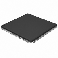
LPC2939FBD208,551 NXP Semiconductors, LPC2939FBD208,551 Datasheet - Page 79

LPC2939FBD208,551
Manufacturer Part Number
LPC2939FBD208,551
Description
IC ARM9 MCU FLASH 768KB 208-LQFP
Manufacturer
NXP Semiconductors
Series
LPC2900r
Datasheet
1.LPC2939FBD208551.pdf
(99 pages)
Specifications of LPC2939FBD208,551
Core Processor
ARM9
Core Size
32-Bit
Speed
125MHz
Connectivity
CAN, EBI/EMI, I²C, LIN, SPI, UART/USART, USB, USB OTG
Peripherals
DMA, POR, PWM, WDT
Number Of I /o
152
Program Memory Size
768KB (768K x 8)
Program Memory Type
FLASH
Eeprom Size
16K x 8
Ram Size
56K x 8
Voltage - Supply (vcc/vdd)
1.71 V ~ 3.6 V
Data Converters
A/D 24x10b
Oscillator Type
Internal
Operating Temperature
-40°C ~ 85°C
Package / Case
208-LQFP
Processor Series
LPC29
Core
ARM968E-S
3rd Party Development Tools
MDK-ARM, RL-ARM, ULINK2
Development Tools By Supplier
OM11027
Package
208LQFP
Device Core
ARM968E-S
Family Name
LPC2900
Operating Supply Voltage
1.8|3.3 V
Data Bus Width
16|32 Bit
Number Of Programmable I/os
160
Interface Type
CAN/I2C/LIN/QSPI/UART/USB
On-chip Adc
24-chx10-bit
Number Of Timers
6
For Use With
568-4787 - BOARD EVAL LPC2939
Lead Free Status / RoHS Status
Lead free / RoHS Compliant
Other names
935287113551
Available stocks
Company
Part Number
Manufacturer
Quantity
Price
Company:
Part Number:
LPC2939FBD208,551
Manufacturer:
NXP Semiconductors
Quantity:
10 000
NXP Semiconductors
Table 42.
V
ground.
[1]
[2]
[3]
[4]
LPC2939_3
Product data sheet
Symbol
T
t
t
Read cycle parameters
t
t
t
t
t
t
t
t
t
Write cycle parameters
t
t
t
t
t
t
t
a(R)int
a(W)int
CSLAV
OELAV
CSLOEL
su(DQ)
h(D)
CSHOEH
BLSLBLSH
OELOEH
BLSLAV
CSHBLSH
CSLWEL
CSLBLSL
WELDV
CSLDV
WELWEH
BLSLBLSH
DD(CORE)
CLCL
All parameters are guaranteed over the virtual junction temperature range by design. Pre-testing is performed at T
temperature on wafer level. Cased products are tested at T
test conditions to cover the specified temperature and power supply voltage range.
When the byte lane select signals are used to connect the write enable input (8 bit devices), t
When the byte lane select signals are used to connect the write enable input (8 bit devices), t
For 16 and 32 bit devices.
[1]
= V
Parameter
clock cycle time
internal read access time
internal write access time
CS LOW to address valid
time
OE LOW to address valid
time
CS LOW to OE LOW time
data input /output set-up
time
data input hold time
CS HIGH to OE HIGH time
BLS LOW to BLS HIGH time
OE LOW to OE HIGH time
BLS LOW to address valid
time
CS HIGH to BLS HIGH time
CS LOW to WE LOW time
CS LOW to BLS LOW time
WE LOW to data valid time
CS LOW to data valid time
WE LOW to WE HIGH time
BLS LOW to BLS HIGH time
External static memory interface dynamic characteristics
DD(OSC_PLL)
9.6 Dynamic characteristics: external static memory
; V
DD(IO)
= 2.7 V to 3.6 V; V
Conditions
All information provided in this document is subject to legal disclaimers.
Rev. 03 — 7 April 2010
DDA(ADC3V3)
[2]
[3]
[4]
amb
Min
8
-
-
5
5 WSTOEN T
-
11
0
-
-
-
-
-
-
-
-
0.5
-
-
= 25 C (final testing). Both pre-testing and final testing use correlated
= 3.0 V to 3.6 V; all voltages are measured with respect to
ARM9 microcontroller with CAN, LIN, and USB
CLCL
-
Typ
-
-
2.5
2.5 WSTOEN T
0 + WSTOEN T
16
2.5
0
(WST1 WSTOEN +1)
T
(WST1 WSTOEN +1)
T
0 + WSTOEN T
0
(WSTWEN + 0.5) T
WSTWEN T
(WSTWEN + 0.5) T
0.1
(WST2 WSTWEN +1)
T
(WST2 - WSTWEN +2)
T
CLCL
CLCL
CLCL
CLCL
CSHBLSH
CSLBLSL
= t
= 0.5 T
CSLWEL
CLCL
CLCL
CLCL
.
LPC2939
CLCL
© NXP B.V. 2010. All rights reserved.
CLCL
amb
CLCL
CLCL
.
= 85 C ambient
Max Unit
100
20.5 ns
24.9 ns
-
-
-
22
5
-
-
-
-
-
-
-
-
0.3
-
-
79 of 99
ns
ns
ns
ns
ns
ns
ns
ns
ns
ns
ns
ns
ns
ns
ns
ns
ns


