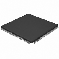
LPC2939FBD208,551 NXP Semiconductors, LPC2939FBD208,551 Datasheet - Page 40

LPC2939FBD208,551
Manufacturer Part Number
LPC2939FBD208,551
Description
IC ARM9 MCU FLASH 768KB 208-LQFP
Manufacturer
NXP Semiconductors
Series
LPC2900r
Datasheet
1.LPC2939FBD208551.pdf
(99 pages)
Specifications of LPC2939FBD208,551
Core Processor
ARM9
Core Size
32-Bit
Speed
125MHz
Connectivity
CAN, EBI/EMI, I²C, LIN, SPI, UART/USART, USB, USB OTG
Peripherals
DMA, POR, PWM, WDT
Number Of I /o
152
Program Memory Size
768KB (768K x 8)
Program Memory Type
FLASH
Eeprom Size
16K x 8
Ram Size
56K x 8
Voltage - Supply (vcc/vdd)
1.71 V ~ 3.6 V
Data Converters
A/D 24x10b
Oscillator Type
Internal
Operating Temperature
-40°C ~ 85°C
Package / Case
208-LQFP
Processor Series
LPC29
Core
ARM968E-S
3rd Party Development Tools
MDK-ARM, RL-ARM, ULINK2
Development Tools By Supplier
OM11027
Package
208LQFP
Device Core
ARM968E-S
Family Name
LPC2900
Operating Supply Voltage
1.8|3.3 V
Data Bus Width
16|32 Bit
Number Of Programmable I/os
160
Interface Type
CAN/I2C/LIN/QSPI/UART/USB
On-chip Adc
24-chx10-bit
Number Of Timers
6
For Use With
568-4787 - BOARD EVAL LPC2939
Lead Free Status / RoHS Status
Lead free / RoHS Compliant
Other names
935287113551
Available stocks
Company
Part Number
Manufacturer
Quantity
Price
Company:
Part Number:
LPC2939FBD208,551
Manufacturer:
NXP Semiconductors
Quantity:
10 000
NXP Semiconductors
LPC2939_3
Product data sheet
6.14.3.1 Pin description
6.14.3 I
6.15 Modulation and Sampling Control SubSystem (MSCSS)
Table 21.
The LPC2939 each contain two I
The I
(SCL) and a serial data line (SDA). Each device is recognized by a unique address and
can operate as either a receiver-only device (e.g., an LCD driver) or as a transmitter with
the capability to both receive and send information (such as memory). Transmitters and/or
receivers can operate in either master or slave mode, depending on whether the chip has
to initiate a data transfer or is only addressed. The I
controlled by more than one bus master connected to it.
The main features if the I
Table 22.
[1]
The Modulation and Sampling Control Subsystem (MSCSS) in the LPC2939 includes four
Pulse-Width Modulators (PWMs), three 10-bit successive approximation Analog-to-Digital
Converters (ADCs) and two timers.
The key features of the MSCSS are:
Symbol
LIN0/1 TXD
LIN0/1 RXD
Symbol
I2C SCL0/1
I2C SDA0/1
2
•
•
•
•
•
•
•
•
•
•
C-bus serial I/O controllers
I
and do not support powering off of individual devices connected to the same bus lines
Easy to configure as master, slave, or master/slave
Programmable clocks allow versatile rate control
Bidirectional data transfer between masters and slaves
Multi-master bus (no central master)
Arbitration between simultaneously transmitting masters without corruption of serial
data on the bus
Serial clock synchronization allows devices with different bit rates to communicate via
one serial bus
Serial clock synchronization can be used as a handshake mechanism to suspend and
resume serial transfer
The I
All I
Note that the pins are not I
2
2
C0 and I
C-bus is bidirectional for inter-IC control using only two wires: a serial clock line
2
C-bus controllers support multiple address recognition and a bus monitor mode
2
C-bus can be used for test and diagnostic purposes
LIN controller pins
I
2
C-bus pins
Pin name
TXDL0/1
RXDL0/1
Pin name
SCL0/1
SDA0/1
2
C1 use standard I/O pins with bit rates of up to 400 kbit/s (Fast I
All information provided in this document is subject to legal disclaimers.
[1]
Rev. 03 — 7 April 2010
2
2
C-bus interfaces are:
C-bus compliant open-drain pins.
Direction
OUT
IN
Direction
I/O
I/O
2
C-bus controllers.
ARM9 microcontroller with CAN, LIN, and USB
Description
LIN channel 0/1 transmit data output
LIN channel 0/1 receive data input
Description
I
I
2
2
C clock input/output
C data input/output
2
C is a multi-master bus, and it can be
LPC2939
© NXP B.V. 2010. All rights reserved.
2
C-bus)
40 of 99


