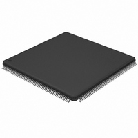
LPC2939FBD208,551 NXP Semiconductors, LPC2939FBD208,551 Datasheet - Page 45

LPC2939FBD208,551
Manufacturer Part Number
LPC2939FBD208,551
Description
IC ARM9 MCU FLASH 768KB 208-LQFP
Manufacturer
NXP Semiconductors
Series
LPC2900r
Datasheet
1.LPC2939FBD208551.pdf
(99 pages)
Specifications of LPC2939FBD208,551
Core Processor
ARM9
Core Size
32-Bit
Speed
125MHz
Connectivity
CAN, EBI/EMI, I²C, LIN, SPI, UART/USART, USB, USB OTG
Peripherals
DMA, POR, PWM, WDT
Number Of I /o
152
Program Memory Size
768KB (768K x 8)
Program Memory Type
FLASH
Eeprom Size
16K x 8
Ram Size
56K x 8
Voltage - Supply (vcc/vdd)
1.71 V ~ 3.6 V
Data Converters
A/D 24x10b
Oscillator Type
Internal
Operating Temperature
-40°C ~ 85°C
Package / Case
208-LQFP
Processor Series
LPC29
Core
ARM968E-S
3rd Party Development Tools
MDK-ARM, RL-ARM, ULINK2
Development Tools By Supplier
OM11027
Package
208LQFP
Device Core
ARM968E-S
Family Name
LPC2900
Operating Supply Voltage
1.8|3.3 V
Data Bus Width
16|32 Bit
Number Of Programmable I/os
160
Interface Type
CAN/I2C/LIN/QSPI/UART/USB
On-chip Adc
24-chx10-bit
Number Of Timers
6
For Use With
568-4787 - BOARD EVAL LPC2939
Lead Free Status / RoHS Status
Lead free / RoHS Compliant
Other names
935287113551
Available stocks
Company
Part Number
Manufacturer
Quantity
Price
Company:
Part Number:
LPC2939FBD208,551
Manufacturer:
NXP Semiconductors
Quantity:
10 000
NXP Semiconductors
LPC2939_3
Product data sheet
6.15.4.3 Clock description
6.15.5 Pulse Width Modulator (PWM)
Table 23.
[1]
[2]
[3]
Remark: The following formula only applies to ADC0:
Voltage variations on VREFP (i.e. those that deviate from voltage variations on the
V
the formula used to determine the conversion result of an input voltage V
Remark: Note that the ADC1 and ADC2 accept an input voltage up to of 3.6 V (see
Table
ADC0 pins are 5 V tolerant.
The ADC modules are clocked from two different sources; CLK_MSCSS_ADCx_APB and
CLK_ADCx (x = 0, 1, or 2), see
CLK_ADCx and CLK_MSCSS_ADCx_APB branch clocks for power management. If an
ADC is unused both its CLK_MSCSS_ADCx_APB and CLK_ADCx can be switched off.
The frequency of all the CLK_MSCSS_ADCx_APB clocks is identical to
CLK_MSCSS_APB since they are derived from the same base clock
BASE_MSCSS_CLK. Likewise the frequency of all the CLK_ADCx clocks is identical
since they are derived from the same base clock BASE_ADC_CLK.
The register interface towards the system bus is clocked by CLK_MSCSS_ADCx_APB.
Control logic for the analog section of the ADC is clocked by CLK_ADCx, see also
Figure
The MSCSS in the LPC2939 includes four PWM modules with the following features.
Symbol
ADC0 IN[7:0]
ADC1/2 IN[7:0]
ADCn_EXTSTART
VREFN
VREFP
V
V
DDA(ADC5V5)
DDA(ADC5V0)
DDA(ADC3V3)
2
-- - V
3
VREFP, VREFN, V
The analog inputs of ADC0 are internally multiplied by a factor of 3.3 / 5. If V
3.3 V, the maximum digital result is 1024 3.3 / 5.
V
DDA(ADC5V0)
IN
34) on the ADC1/2 IN pins. If the ADC is not used, the pins are 5 V tolerant. The
9.
–
1
-- - V
2
Analog to digital converter pins
DDA ADC5V0
pin) are visible as variations in the measurement result.
and V
All information provided in this document is subject to legal disclaimers.
DDA(ADC3V3)
DDA(ADC3V3)
Pin name
IN0[7:0]
IN1/2[7:0]
CAP1[n]
VREFN
VREFP
V
V
DDA(ADC5V0)
DDA(ADC3V3)
Rev. 03 — 7 April 2010
+
1
-- - V
2
must be connected for the 5 V ADC0 to operate properly.
must be set as follows: V
DDA ADC3V3
[1]
Section
Direction Description
IN
IN
IN
IN
IN
IN
IN
ARM9 microcontroller with CAN, LIN, and USB
6.7.2. Note that each ADC has its own
analog input for 5.0 V ADC0, channel 7 to
channel 0
analog input for 3.3 V ADC1/2, channel 7 to
channel 0
ADC external start-trigger input (n is 0, 1, or 2)
ADC LOW reference level
ADC HIGH reference level
5 V high-power supply and HIGH reference for
ADC0. Connect to clean 5 V as HIGH reference.
May also be connected to 3.3 V if 3.3 V
measurement range for ADC0 is needed.
ADC1 and ADC2 3.3 V supply (also used for
ADC0).
------------------------------------------- -
V
VREFP
DDA(ADC5V0)
[3]
1024
–
V
VREFN
= V
DDA(ADC3V3)
DDA(ADC5V0)
Equation 3
LPC2939
© NXP B.V. 2010. All rights reserved.
1.5.
IN
is connected to
on ADC0:
shows
[2][3]
45 of 99
(3)


