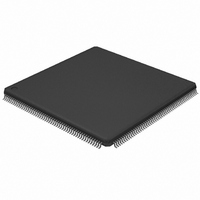
LPC2939FBD208,551 NXP Semiconductors, LPC2939FBD208,551 Datasheet - Page 39

LPC2939FBD208,551
Manufacturer Part Number
LPC2939FBD208,551
Description
IC ARM9 MCU FLASH 768KB 208-LQFP
Manufacturer
NXP Semiconductors
Series
LPC2900r
Datasheet
1.LPC2939FBD208551.pdf
(99 pages)
Specifications of LPC2939FBD208,551
Core Processor
ARM9
Core Size
32-Bit
Speed
125MHz
Connectivity
CAN, EBI/EMI, I²C, LIN, SPI, UART/USART, USB, USB OTG
Peripherals
DMA, POR, PWM, WDT
Number Of I /o
152
Program Memory Size
768KB (768K x 8)
Program Memory Type
FLASH
Eeprom Size
16K x 8
Ram Size
56K x 8
Voltage - Supply (vcc/vdd)
1.71 V ~ 3.6 V
Data Converters
A/D 24x10b
Oscillator Type
Internal
Operating Temperature
-40°C ~ 85°C
Package / Case
208-LQFP
Processor Series
LPC29
Core
ARM968E-S
3rd Party Development Tools
MDK-ARM, RL-ARM, ULINK2
Development Tools By Supplier
OM11027
Package
208LQFP
Device Core
ARM968E-S
Family Name
LPC2900
Operating Supply Voltage
1.8|3.3 V
Data Bus Width
16|32 Bit
Number Of Programmable I/os
160
Interface Type
CAN/I2C/LIN/QSPI/UART/USB
On-chip Adc
24-chx10-bit
Number Of Timers
6
For Use With
568-4787 - BOARD EVAL LPC2939
Lead Free Status / RoHS Status
Lead free / RoHS Compliant
Other names
935287113551
Available stocks
Company
Part Number
Manufacturer
Quantity
Price
Company:
Part Number:
LPC2939FBD208,551
Manufacturer:
NXP Semiconductors
Quantity:
10 000
NXP Semiconductors
LPC2939_3
Product data sheet
6.14.1.1 Global acceptance filter
6.14.1.2 Pin description
6.14.2.1 Pin description
6.14.2 LIN
The global acceptance filter provides look-up of received identifiers - called acceptance
filtering in CAN terminology - for all the CAN controllers. It includes a CAN ID look-up table
memory, in which software maintains one to five sections of identifiers. The CAN ID
look-up table memory is 2 kB large (512 words, each of 32 bits). It can contain up to 1024
standard frame identifiers or 512 extended frame identifiers or a mixture of both types. It is
also possible to define identifier groups for standard and extended message formats.
The two CAN controllers in the LPC2939 have the pins listed below. The CAN pins are
combined with other functions on the port pins of the LPC2939.
pins (x runs from 0 to 1).
Table 20.
The LPC2939 contain two LIN 2.0 master controllers. These can be used as dedicated
LIN 2.0 master controllers with additional support for sync break generation and with
hardware implementation of the LIN protocol according to spec 2.0.
Remark: Both LIN channels can be also configured as UART channels.
The key features are:
The two LIN 2.0 master controllers in the LPC2939 have the pins listed below. The LIN
pins are combined with other functions on the port pins of the LPC2939.
the LIN pins. For more information see
Symbol
CANx TXD
CANx RXD
•
•
•
•
•
•
•
•
•
•
•
•
•
Listen-only mode (no acknowledge; no active error flags)
Reception of ‘own’ messages (self-reception request)
Full CAN mode for message reception
Complete LIN 2.0 message handling and transfer
One interrupt per LIN message
Slave response time-out detection
Programmable sync-break length
Automatic sync-field and sync-break generation
Programmable inter-byte space
Hardware or software parity generation
Automatic checksum generation
Fault confinement
Fractional baud rate generator
CAN pins
Pin name
TXDC0/1
RXDC0/1
All information provided in this document is subject to legal disclaimers.
Rev. 03 — 7 April 2010
Direction
OUT
IN
Ref. 1
ARM9 microcontroller with CAN, LIN, and USB
Description
CAN channel x transmit data output
CAN channel x receive data input
subsection 3.43, LIN master controller.
Table 20
LPC2939
© NXP B.V. 2010. All rights reserved.
Table 21
shows the CAN
shows
39 of 99


