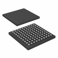
ATSAM3S4CA-CU Atmel, ATSAM3S4CA-CU Datasheet - Page 221

ATSAM3S4CA-CU
Manufacturer Part Number
ATSAM3S4CA-CU
Description
IC MCU 32BIT 256KB FLASH 100BGA
Manufacturer
Atmel
Series
SAM3Sr
Specifications of ATSAM3S4CA-CU
Core Processor
ARM® Cortex-M3™
Core Size
32-Bit
Speed
64MHz
Connectivity
EBI/EMI, I²C, MMC, SPI, SSC, UART/USART, USB
Peripherals
Brown-out Detect/Reset, DMA, I²S, POR, PWM, WDT
Number Of I /o
79
Program Memory Size
256KB (256K x 8)
Program Memory Type
FLASH
Ram Size
48K x 8
Voltage - Supply (vcc/vdd)
1.62 V ~ 1.95 V
Data Converters
A/D 16x10/12b, D/A 2x12b
Oscillator Type
Internal
Operating Temperature
-40°C ~ 85°C
Package / Case
100-LFBGA
Processor Series
ATSAM3x
Core
ARM Cortex M3
3rd Party Development Tools
JTRACE-CM3, MDK-ARM, RL-ARM, ULINK2
Development Tools By Supplier
ATSAM3S-EK
Package
100LFBGA
Device Core
ARM Cortex M3
Family Name
AT91
Maximum Speed
64 MHz
Operating Supply Voltage
1.8|3.3 V
Data Bus Width
32 Bit
Number Of Programmable I/os
79
Interface Type
I2C/I2S/SPI/UART/USART/USB
On-chip Adc
16-chx12-bit
On-chip Dac
2-chx12-bit
Number Of Timers
6
Lead Free Status / RoHS Status
Lead free / RoHS Compliant
Eeprom Size
-
Lead Free Status / Rohs Status
Details
Available stocks
Company
Part Number
Manufacturer
Quantity
Price
Company:
Part Number:
ATSAM3S4CA-CU
Manufacturer:
SANYO
Quantity:
1 000
- Current page: 221 of 1118
- Download datasheet (24Mb)
11.5.6.2
11.5.6.3
11.5.7
11.5.7.1
6500C–ATARM–8-Feb-11
IEEE
Asynchronous Mode
5.4.3. How to Configure the TPIU
JTAG Boundary-scan Register
®
1149.1 JTAG Boundary Scan
The TPIU is configured in asynchronous mode, trace data are output using the single TRAC-
ESWO pin. The TRACESWO signal is multiplexed with the TDO signal of the JTAG Debug Port.
As a consequence, asynchronous trace mode is only available when the Serial Wire Debug
mode is selected since TDO signal is used in JTAG debug mode.
Two encoding formats are available for the single pin output:
This example only concerns the asynchronous trace mode.
IEEE 1149.1 JTAG Boundary Scan allows pin-level access independent of the device packaging
technology.
IEEE 1149.1 JTAG Boundary Scan is enabled when TST is tied to low while JTAGSEL is high
during power-up and must be kept in this state during the whole boundary scan operation.
VDDCORE must be externally supplied between 1.8V and 1.95V. The SAMPLE, EXTEST and
BYPASS functions are implemented. In SWD/JTAG debug mode, the ARM processor responds
with a non-JTAG chip ID that identifies the processor. This is not IEEE 1149.1 JTAG-compliant.
It is not possible to switch directly between JTAG Boundary Scan and SWJ Debug Port opera-
tions. A chip reset must be performed after JTAGSEL is changed.
A Boundary-scan Descriptor Language (BSDL) file is provided on
test.
The Boundary-scan Register (BSR) contains a number of bits which correspond to active pins
and associated control signals.
Each SAM3 input/output pin corresponds to a 3-bit register in the BSR. The OUTPUT bit con-
tains data that can be forced on the pad. The INPUT bit facilitates the observability of data
applied to the pad. The CONTROL bit selects the direction of the pad.
For more information, please refer to BDSL files available for the SAM3 Series.
• Manchester encoded stream. This is the reset value.
• NRZ_based UART byte structure
• Set the TRCENA bit to 1 into the Debug Exception and Monitor Register (0xE000EDFC) to
• Write 0x2 into the Selected Pin Protocol Register
• Write 0x100 into the Formatter and Flush Control Register
• Set the suitable clock prescaler value into the Async Clock Prescaler Register to scale the
enable the use of trace and debug blocks.
baud rate of the asynchronous output (this can be done automatically by the debugging tool).
– Select the Serial Wire Output – NRZ
SAM3S Preliminary
Atmel’s web site
to set up the
221
Related parts for ATSAM3S4CA-CU
Image
Part Number
Description
Manufacturer
Datasheet
Request
R

Part Number:
Description:
KIT EVAL FOR ATSAM3S4C
Manufacturer:
Atmel
Datasheet:

Part Number:
Description:
Development Boards & Kits - ARM EVAL KIT SAM3S8 & SAM3SD8 series
Manufacturer:
Atmel
Datasheet:

Part Number:
Description:
AT91 ARM Cortex M3-based Processor
Manufacturer:
ATMEL [ATMEL Corporation]
Datasheet:

Part Number:
Description:
DEV KIT FOR AVR/AVR32
Manufacturer:
Atmel
Datasheet:

Part Number:
Description:
INTERVAL AND WIPE/WASH WIPER CONTROL IC WITH DELAY
Manufacturer:
ATMEL Corporation
Datasheet:

Part Number:
Description:
Low-Voltage Voice-Switched IC for Hands-Free Operation
Manufacturer:
ATMEL Corporation
Datasheet:

Part Number:
Description:
MONOLITHIC INTEGRATED FEATUREPHONE CIRCUIT
Manufacturer:
ATMEL Corporation
Datasheet:

Part Number:
Description:
AM-FM Receiver IC U4255BM-M
Manufacturer:
ATMEL Corporation
Datasheet:

Part Number:
Description:
Monolithic Integrated Feature Phone Circuit
Manufacturer:
ATMEL Corporation
Datasheet:

Part Number:
Description:
Multistandard Video-IF and Quasi Parallel Sound Processing
Manufacturer:
ATMEL Corporation
Datasheet:

Part Number:
Description:
High-performance EE PLD
Manufacturer:
ATMEL Corporation
Datasheet:

Part Number:
Description:
8-bit Flash Microcontroller
Manufacturer:
ATMEL Corporation
Datasheet:


