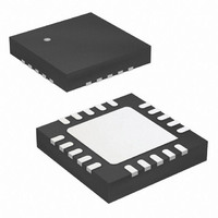
ATTINY84-15MZ Atmel, ATTINY84-15MZ Datasheet - Page 98

ATTINY84-15MZ
Manufacturer Part Number
ATTINY84-15MZ
Description
MCU AVR 8K FLASH 15MHZ 20-QFN
Manufacturer
Atmel
Series
AVR® ATtinyr
Specifications of ATTINY84-15MZ
Package / Case
20-QFN Exposed Pad
Voltage - Supply (vcc/vdd)
2.7 V ~ 5.5 V
Operating Temperature
-40°C ~ 125°C
Speed
16MHz
Number Of I /o
12
Eeprom Size
512 x 8
Core Processor
AVR
Program Memory Type
FLASH
Ram Size
512 x 8
Program Memory Size
8KB (8K x 8)
Data Converters
A/D 8x10b
Oscillator Type
Internal
Peripherals
Brown-out Detect/Reset, POR, PWM, WDT
Connectivity
USI
Core Size
8-Bit
Processor Series
ATTINY8x
Core
AVR8
Data Bus Width
8 bit
Data Ram Size
512 B
Interface Type
SPI, UART
Maximum Clock Frequency
16 MHz
Number Of Programmable I/os
12
Number Of Timers
2
Maximum Operating Temperature
+ 85 C
Mounting Style
SMD/SMT
3rd Party Development Tools
EWAVR, EWAVR-BL
Development Tools By Supplier
ATAVRDRAGON, ATSTK500, ATSTK600, ATAVRISP2, ATAVRONEKIT
Minimum Operating Temperature
- 40 C
On-chip Adc
10 bit, 8 Channel
Lead Free Status / RoHS Status
Lead free / RoHS Compliant
Available stocks
Company
Part Number
Manufacturer
Quantity
Price
Company:
Part Number:
ATTINY84-15MZ
Manufacturer:
ATMEL
Quantity:
480
Part Number:
ATTINY84-15MZ
Manufacturer:
ATMEL/爱特梅尔
Quantity:
20 000
14.6.1
14.6.2
14.6.3
98
Atmel ATtiny24/44/84 [Preliminary]
Input Capture Trigger Source
Noise Canceller
Using the Input Capture Unit
The ICR1 register can only be written when using a waveform generation mode that utilizes
the ICR1 register for defining the counter's top value. In these cases the waveform generation
mode (WGM13:0) bits must be set before the top value can be written to the ICR1 register.
When writing the ICR1 register, the high byte must be written to the ICR1H I/O location before
the low byte is written to ICR1L.
For more information on how to access the 16-bit registers refer to
ters” on page
The main trigger source for the input capture unit is the input capture pin (ICP1). Timer/coun-
ter 1 can alternatively use the analog comparator output as trigger source for the input capture
unit. The analog comparator is selected as trigger source by setting the analog comparator
input capture (ACIC) bit in the analog comparator control and status register (ACSR). Be
aware that changing the trigger source can trigger a capture. The input capture flag must,
therefore, be cleared after the change.
Both the input capture pin (ICP1) and the analog comparator output (ACO) are sampled using
the same technique as for the T1 pin
identical. However, when the noise canceller is enabled, additional logic is inserted before the
edge detector, which increases the delay by four system clock cycles. Note that the inputs of
the noise canceller and edge detector are always enabled unless the timer/counter is set in a
waveform generation mode that uses ICR1 to define top.
An input capture can be triggered by software by controlling the port of the ICP1 pin.
The noise canceller improves noise immunity by using a simple digital filtering scheme. The
noise canceller input is monitored over four samples, and all four must be equal to change the
output, which in turn is used by the edge detector.
The noise canceller is enabled by setting the input capture noise canceller (ICNC1) bit in
timer/counter control register B (TCCR1B). When enabled, the noise canceller introduces an
additional four system clock cycles of delay between a change applied to the input and the
update of the ICR1 register. The noise canceller uses the system clock, and is, therefore, not
affected by the prescaler.
The main challenge when using the input capture unit is to assign enough processor capacity
for handling the incoming events. The time between two events is critical. If the processor has
not read the captured value in the ICR1 register before the next event occurs, the ICR1 will be
overwritten with a new value. In this case the result of the capture will be incorrect.
When using the input capture interrupt, the ICR1 register should be read as early in the inter-
rupt handler routine as possible. Even though the input capture interrupt has relatively high
priority, the maximum interrupt response time is dependent on the maximum number of clock
cycles it takes to handle any of the other interrupt requests.
Using the input capture unit in any mode of operation when the top value (resolution) is
actively changed during operation is not recommended.
93.
(Figure 15-1 on page
119). The edge detector is also
“Accessing 16-bit Regis-
7701D–AVR–09/10


