ATTINY84-15MZ Atmel, ATTINY84-15MZ Datasheet - Page 153
ATTINY84-15MZ
Manufacturer Part Number
ATTINY84-15MZ
Description
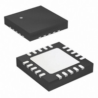
MCU AVR 8K FLASH 15MHZ 20-QFN
Manufacturer
Atmel
Series
AVR® ATtinyr
Specifications of ATTINY84-15MZ
Package / Case
20-QFN Exposed Pad
Voltage - Supply (vcc/vdd)
2.7 V ~ 5.5 V
Operating Temperature
-40°C ~ 125°C
Speed
16MHz
Number Of I /o
12
Eeprom Size
512 x 8
Core Processor
AVR
Program Memory Type
FLASH
Ram Size
512 x 8
Program Memory Size
8KB (8K x 8)
Data Converters
A/D 8x10b
Oscillator Type
Internal
Peripherals
Brown-out Detect/Reset, POR, PWM, WDT
Connectivity
USI
Core Size
8-Bit
Processor Series
ATTINY8x
Core
AVR8
Data Bus Width
8 bit
Data Ram Size
512 B
Interface Type
SPI, UART
Maximum Clock Frequency
16 MHz
Number Of Programmable I/os
12
Number Of Timers
2
Maximum Operating Temperature
+ 85 C
Mounting Style
SMD/SMT
3rd Party Development Tools
EWAVR, EWAVR-BL
Development Tools By Supplier
ATAVRDRAGON, ATSTK500, ATSTK600, ATAVRISP2, ATAVRONEKIT
Minimum Operating Temperature
- 40 C
On-chip Adc
10 bit, 8 Channel
Lead Free Status / RoHS Status
Lead free / RoHS Compliant
Available stocks
Company
Part Number
Manufacturer
Quantity
Price
Company:

Part Number:
ATTINY84-15MZ
Manufacturer:
ATMEL
Quantity:
480
Part Number:
ATTINY84-15MZ
Manufacturer:
ATMEL/爱特梅尔
Quantity:
20 000


18.10.4
7701D–AVR–09/10
ADCSRB – ADC Control and Status Register B
• Bits 7 – BIN: Bipolar Input Mode
The gain stage is working in the unipolar mode by default, but the bipolar mode can be
selected by writing the BIN bit in the ADCSRB register. In the unipolar mode, only one-sided
conversions are supported, and the voltage on the positive input must always be larger than
the voltage on the negative input. Otherwise, the result is saturated to the voltage reference. In
the bipolar mode, two-sided conversions are supported, and the result is represented in two's
complement form. In unipolar mode, the resolution is 10 bits, and in bipolar mode the resolu-
tion is 9 bits + 1 sign bit.
• Bit 6 – ACME: Analog Comparator Multiplexer Enable
See
• Bit 5 – Res: Reserved Bit
This bit is reserved bit in the Atmel® ATtiny24/44/84, and will always read as what was written
there.
• Bit 4 – ADLAR: ADC Left Adjust Result
The ADLAR bit affects the presentation of the ADC conversion result in the ADC data register.
Write logical one to ADLAR to left adjust the result. Otherwise, the result is right adjusted.
Changing the ADLAR bit will affect the ADC data register immediately, regardless of any
ongoing conversions. For a complete description of this bit, see
Data Register” on page
• Bit 3 – Res: Reserved Bit
This bit is reserved bit in the Atmel
there.
• Bits 2:0 – ADTS2:0: ADC Auto Trigger Source
If ADATE in ADCSRA is written to logical one, the value of these bits selects which source will
trigger an ADC conversion. If ADATE is cleared, the ADTS2:0 settings will have no effect. A
conversion will be triggered by the rising edge of the selected interrupt flag. Note that switch-
ing from a trigger source that is cleared to a trigger source that is set will generate a positive
edge on the trigger signal. If ADEN in ADCSRA is set, this will start a conversion. Switching to
free running mode (ADTS[2:0]=0) will not cause a trigger event, even if the ADC Interrupt Flag
is set.
Bit
0x03 (0x23)
Read/Write
Initial Value
“ADCSRB – ADC Control and Status Register B” on page
R/W
BIN
7
0
152.
ACME
R/W
6
0
Atmel ATtiny24/44/84 [Preliminary]
R/W
®
5
–
0
ATtiny24/44/84, and will always read as what was written
ADLAR
R/W
4
0
R/W
3
–
0
ADTS2
R/W
2
0
134.
“ADCL and ADCH – ADC
ADTS1
R/W
1
0
ADTS0
R/W
0
0
ADCSRB
153
Related parts for ATTINY84-15MZ
Image
Part Number
Description
Manufacturer
Datasheet
Request
R

Part Number:
Description:
Manufacturer:
Atmel Corporation
Datasheet:
Part Number:
Description:
Manufacturer:
Atmel Corporation
Datasheet:

Part Number:
Description:
IC MCU AVR 8K FLASH 20MHZ 20-QFN
Manufacturer:
Atmel
Datasheet:

Part Number:
Description:
MCU AVR 8K ISP FLASH 2.7V 14SOIC
Manufacturer:
Atmel
Datasheet:

Part Number:
Description:
IC MCU AVR 8K FLASH 20MHZ 14-DIP
Manufacturer:
Atmel
Datasheet:

Part Number:
Description:
MCU AVR 8KB FLASH 10MHZ 14SOIC
Manufacturer:
Atmel
Datasheet:
Part Number:
Description:
MCU AVR 8KB FLASH 20MHZ 20QFN
Manufacturer:
Atmel
Datasheet:

Part Number:
Description:
DEV KIT FOR AVR/AVR32
Manufacturer:
Atmel
Datasheet:
Part Number:
Description:
INTERVAL AND WIPE/WASH WIPER CONTROL IC WITH DELAY
Manufacturer:
ATMEL Corporation
Datasheet:
Part Number:
Description:
Low-Voltage Voice-Switched IC for Hands-Free Operation
Manufacturer:
ATMEL Corporation
Datasheet:
Part Number:
Description:
MONOLITHIC INTEGRATED FEATUREPHONE CIRCUIT
Manufacturer:
ATMEL Corporation
Datasheet:
Part Number:
Description:
AM-FM Receiver IC U4255BM-M
Manufacturer:
ATMEL Corporation
Datasheet:
Part Number:
Description:
Monolithic Integrated Feature Phone Circuit
Manufacturer:
ATMEL Corporation
Datasheet:
Part Number:
Description:
Multistandard Video-IF and Quasi Parallel Sound Processing
Manufacturer:
ATMEL Corporation
Datasheet: