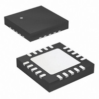
ATTINY84-15MZ Atmel, ATTINY84-15MZ Datasheet - Page 172

ATTINY84-15MZ
Manufacturer Part Number
ATTINY84-15MZ
Description
MCU AVR 8K FLASH 15MHZ 20-QFN
Manufacturer
Atmel
Series
AVR® ATtinyr
Specifications of ATTINY84-15MZ
Package / Case
20-QFN Exposed Pad
Voltage - Supply (vcc/vdd)
2.7 V ~ 5.5 V
Operating Temperature
-40°C ~ 125°C
Speed
16MHz
Number Of I /o
12
Eeprom Size
512 x 8
Core Processor
AVR
Program Memory Type
FLASH
Ram Size
512 x 8
Program Memory Size
8KB (8K x 8)
Data Converters
A/D 8x10b
Oscillator Type
Internal
Peripherals
Brown-out Detect/Reset, POR, PWM, WDT
Connectivity
USI
Core Size
8-Bit
Processor Series
ATTINY8x
Core
AVR8
Data Bus Width
8 bit
Data Ram Size
512 B
Interface Type
SPI, UART
Maximum Clock Frequency
16 MHz
Number Of Programmable I/os
12
Number Of Timers
2
Maximum Operating Temperature
+ 85 C
Mounting Style
SMD/SMT
3rd Party Development Tools
EWAVR, EWAVR-BL
Development Tools By Supplier
ATAVRDRAGON, ATSTK500, ATSTK600, ATAVRISP2, ATAVRONEKIT
Minimum Operating Temperature
- 40 C
On-chip Adc
10 bit, 8 Channel
Lead Free Status / RoHS Status
Lead free / RoHS Compliant
Available stocks
Company
Part Number
Manufacturer
Quantity
Price
Company:
Part Number:
ATTINY84-15MZ
Manufacturer:
ATMEL
Quantity:
480
Part Number:
ATTINY84-15MZ
Manufacturer:
ATMEL/爱特梅尔
Quantity:
20 000
- Current page: 172 of 225
- Download datasheet (4Mb)
21.8.3
21.8.4
172
Atmel ATtiny24/44/84 [Preliminary]
Chip Erase
Programming the Flash
The Chip Erase will erase the Flash and EEPROM
bits are not reset until the program memory has been completely erased. The fuse bits are not
changed. A chip erase must be performed before the flash and/or EEPROM are
reprogrammed.
Note:
1. Load "Chip Erase" command (see
2. Wait after Instr. 3 until SDO goes high for the “Chip Erase” cycle to finish.
3. Load "No Operation" command.
The Flash is organized in pages, see
the program data are latched into a page buffer. This allows one page of program data to be
programmed simultaneously. The following procedure describes how to program the entire
flash memory:
1. Load "Write Flash" command (see
2. Load Flash Page Buffer.
3. Load Flash High Address and Program Page. Wait after Instr. 3 until SDO goes high for
4. Repeat 2 and 3 until the entire flash is programmed, or until all data has been
5. End page programming by loading "No Operation" command.
When writing or reading serial data to the Atmel
ing edge of the serial clock. See
22-9 on page 185
Figure 21-4. Addressing the Flash which is Organized in Pages
the “Page Programming” cycle to finish.
programmed.
1. The EEPROM memory is preserved during Chip Erase if the EESAVE Fuse is programmed.
PROGRAM MEMORY
PROGRAM
COUNTER
PAGE
for details.
PAGE ADDRESS
WITHIN THE FLASH
PCMSB
PCPAGE
Figure 22-5 on page
“Page Size” on page
Table 21-15 on page
Table 21-15 on page
PAGEMSB
PCWORD
WORD ADDRESS
WITHIN A PAGE
®
ATtiny24/44/84, data are clocked on the ris-
(1)
185,
memories, as well as lock bits. The lock
INSTRUCTION WORD
Figure 21-3 on page 170
165. When programming the flash,
PAGE
174).
174).
PCWORD[PAGEMSB:0]:
00
01
02
PAGEEND
7701D–AVR–09/10
and
Table
Related parts for ATTINY84-15MZ
Image
Part Number
Description
Manufacturer
Datasheet
Request
R

Part Number:
Description:
Manufacturer:
Atmel Corporation
Datasheet:

Part Number:
Description:
Manufacturer:
Atmel Corporation
Datasheet:

Part Number:
Description:
IC MCU AVR 8K FLASH 20MHZ 20-QFN
Manufacturer:
Atmel
Datasheet:

Part Number:
Description:
MCU AVR 8K ISP FLASH 2.7V 14SOIC
Manufacturer:
Atmel
Datasheet:

Part Number:
Description:
IC MCU AVR 8K FLASH 20MHZ 14-DIP
Manufacturer:
Atmel
Datasheet:

Part Number:
Description:
MCU AVR 8KB FLASH 10MHZ 14SOIC
Manufacturer:
Atmel
Datasheet:

Part Number:
Description:
MCU AVR 8KB FLASH 20MHZ 20QFN
Manufacturer:
Atmel
Datasheet:

Part Number:
Description:
DEV KIT FOR AVR/AVR32
Manufacturer:
Atmel
Datasheet:

Part Number:
Description:
INTERVAL AND WIPE/WASH WIPER CONTROL IC WITH DELAY
Manufacturer:
ATMEL Corporation
Datasheet:

Part Number:
Description:
Low-Voltage Voice-Switched IC for Hands-Free Operation
Manufacturer:
ATMEL Corporation
Datasheet:

Part Number:
Description:
MONOLITHIC INTEGRATED FEATUREPHONE CIRCUIT
Manufacturer:
ATMEL Corporation
Datasheet:

Part Number:
Description:
AM-FM Receiver IC U4255BM-M
Manufacturer:
ATMEL Corporation
Datasheet:

Part Number:
Description:
Monolithic Integrated Feature Phone Circuit
Manufacturer:
ATMEL Corporation
Datasheet:

Part Number:
Description:
Multistandard Video-IF and Quasi Parallel Sound Processing
Manufacturer:
ATMEL Corporation
Datasheet:


