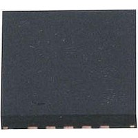
ATTINY25-15MZ Atmel, ATTINY25-15MZ Datasheet - Page 122

ATTINY25-15MZ
Manufacturer Part Number
ATTINY25-15MZ
Description
MCU AVR 2K FLASH 15MHZ 20-QFN
Manufacturer
Atmel
Series
AVR® ATtinyr
Datasheet
1.ATTINY25-15MZ.pdf
(196 pages)
Specifications of ATTINY25-15MZ
Package / Case
20-QFN
Voltage - Supply (vcc/vdd)
2.7 V ~ 5.5 V
Operating Temperature
-40°C ~ 125°C
Speed
16MHz
Number Of I /o
6
Eeprom Size
128 x 8
Core Processor
AVR
Program Memory Type
FLASH
Ram Size
128 x 8
Program Memory Size
2KB (2K x 8)
Data Converters
A/D 4x10b
Oscillator Type
Internal
Peripherals
Brown-out Detect/Reset, POR, PWM, WDT
Connectivity
USI
Core Size
8-Bit
Processor Series
ATTINY2x
Core
AVR8
Data Bus Width
8 bit
Data Ram Size
128 B
Interface Type
UART, SPI, USI
Maximum Clock Frequency
16 MHz
Number Of Programmable I/os
6
Number Of Timers
2
Maximum Operating Temperature
+ 85 C
Mounting Style
SMD/SMT
3rd Party Development Tools
EWAVR, EWAVR-BL
Development Tools By Supplier
ATAVRDRAGON, ATSTK500, ATSTK600, ATAVRISP2, ATAVRONEKIT
Minimum Operating Temperature
- 40 C
On-chip Adc
10 bit, 4 Channel
Data Rom Size
128 B
A/d Bit Size
10 bit
A/d Channels Available
4
Height
0.75 mm
Length
4 mm
Supply Voltage (max)
5.5 V
Supply Voltage (min)
2.7 V
Width
4 mm
Lead Free Status / RoHS Status
Lead free / RoHS Compliant
18.7.3
18.7.4
122
ATtiny25/45/85
Bipolar Differential Conversion
Temperature Measurement (Preliminary description)
where V
and V
124). The voltage on the positive pin must always be larger than the voltage on the negative pin
or otherwise the voltage difference is saturated to zero. The result is presented in one-sided
form, from 0x000 (0d) to 0x3FF (+1023d). The GAIN is either 1x or 20x.
As default the ADC converter operates in the unipolar input mode, but the bipolar input mode
can be selected by writting the BIN bit in the ADCSRB to one. In the bipolar input mode
two-sided voltage differences are allowed and thus the voltage on the negative input pin can
also be larger than the voltage on the positive input pin. If differential channels and a bipolar
input mode are used, the result is
where V
and V
0x200 (-512d) through 0x000 (+0d) to 0x1FF (+511d). The GAIN is either 1x or 20x.
However, if the signal is not bipolar by nature (9 bits + sign as the 10th bit), this scheme loses
one bit of the converter dynamic range. Then, if the user wants to perform the conversion with
the maximum dynamic range, the user can perform a quick polarity check of the result and use
the unipolar differential conversion with selectable differential input pairs (see the Input Polarity
Reversal mode ie. the IPR bit in the ADCSRB register on page 135). When the polarity check is
performed, it is sufficient to read the MSB of the result (ADC9 in ADCH). If the bit is one, the
result is negative, and if this bit is zero, the result is positive.
The temperature measurement is based on an on-chip temperature sensor that is coupled to a
single ended ADC4 channel. Selecting the ADC4 channel by writing the MUX3..0 bits in ADMUX
register to “1111” enables the temperature sensor. The internal 1.1V voltage reference must
also be selected for the ADC voltage reference source in the temperature sensor measurement.
When the temperature sensor is enabled, the ADC converter can be used in single conversion
mode to measure the voltage over the temperature sensor.
The measured voltage has a linear relationship to the temperature as described in Table 51. The
voltage sensitivity is approximately 1 mV /
is +/-
Table 18-2.
ADC
Temperature / °C
10°
REF
REF
Voltage / mV
=
POS
POS
-------------------------------------------------------
C after bandgap calibration.
V
the selected voltage reference. The result is presented in two’s complement form, from
the selected voltage reference (see
POS
is the voltage on the positive input pin, V
is the voltage on the positive input pin, V
Temperature vs. Sensor Output Voltage (Typical Case)
–
V
V
REF
NEG
-45°C
512
242 mV
GAIN
°
C and the accuracy of the temperature measurement
Table 18-3 on page 123
+25°C
NEG
NEG
314 mv
the voltage on the negative input pin,
the voltage on the negative input pin,
and
+105°C
403 mV
Table 18-4 on page
7598H–AVR–07/09


