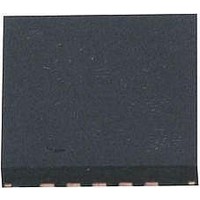
ATTINY25-15MZ Atmel, ATTINY25-15MZ Datasheet - Page 108

ATTINY25-15MZ
Manufacturer Part Number
ATTINY25-15MZ
Description
MCU AVR 2K FLASH 15MHZ 20-QFN
Manufacturer
Atmel
Series
AVR® ATtinyr
Datasheet
1.ATTINY25-15MZ.pdf
(196 pages)
Specifications of ATTINY25-15MZ
Package / Case
20-QFN
Voltage - Supply (vcc/vdd)
2.7 V ~ 5.5 V
Operating Temperature
-40°C ~ 125°C
Speed
16MHz
Number Of I /o
6
Eeprom Size
128 x 8
Core Processor
AVR
Program Memory Type
FLASH
Ram Size
128 x 8
Program Memory Size
2KB (2K x 8)
Data Converters
A/D 4x10b
Oscillator Type
Internal
Peripherals
Brown-out Detect/Reset, POR, PWM, WDT
Connectivity
USI
Core Size
8-Bit
Processor Series
ATTINY2x
Core
AVR8
Data Bus Width
8 bit
Data Ram Size
128 B
Interface Type
UART, SPI, USI
Maximum Clock Frequency
16 MHz
Number Of Programmable I/os
6
Number Of Timers
2
Maximum Operating Temperature
+ 85 C
Mounting Style
SMD/SMT
3rd Party Development Tools
EWAVR, EWAVR-BL
Development Tools By Supplier
ATAVRDRAGON, ATSTK500, ATSTK600, ATAVRISP2, ATAVRONEKIT
Minimum Operating Temperature
- 40 C
On-chip Adc
10 bit, 4 Channel
Data Rom Size
128 B
A/d Bit Size
10 bit
A/d Channels Available
4
Height
0.75 mm
Length
4 mm
Supply Voltage (max)
5.5 V
Supply Voltage (min)
2.7 V
Width
4 mm
Lead Free Status / RoHS Status
Lead free / RoHS Compliant
- Current page: 108 of 196
- Download datasheet (4Mb)
17. Analog Comparator
17.1
17.2
108
ADC Control and Status Register B – ADCSRB
Analog Comparator Control and Status Register – ACSR
ATtiny25/45/85
The Analog Comparator compares the input values on the positive pin AIN0 and negative pin
AIN1. When the voltage on the positive pin AIN0 is higher than the voltage on the negative pin
AIN1, the Analog Comparator output, ACO, is set. The comparator can trigger a separate inter-
rupt, exclusive to the Analog Comparator. The user can select Interrupt triggering on comparator
output rise, fall or toggle. A block diagram of the comparator and its surrounding logic is shown
in
Figure 17-1. Analog Comparator Block Diagram
Notes:
• Bit 6 – ACME: Analog Comparator Multiplexer Enable
When this bit is written logic one and the ADC is switched off (ADEN in ADCSRA is zero), the
ADC multiplexer selects the negative input to the Analog Comparator. When this bit is written
logic zero, AIN1 is applied to the negative input of the Analog Comparator. For a detailed
description of this bit, see
• Bit 7 – ACD: Analog Comparator Disable
When this bit is written logic one, the power to the Analog Comparator is switched off. This bit
can be set at any time to turn off the Analog Comparator.
Bit
Read/Write
Initial Value
Bit
Read/Write
Initial Value
Figure
ADC MULTIPLEXER
1. See
2. Refer to
17-1.
REFERENCE
ACME
ADEN
BANDGAP
OUTPUT
placement.
Table 17-2 on page
ACD
R/W
(1)
BIN
R
7
0
7
0
Figure 1-1 on page 2
ACBG
ACBG
ACME
R/W
R/W
“Analog Comparator Multiplexed Input” on page
6
0
6
0
110.
ACO
N/A
IPR
R
5
R
5
0
and
Table 10-5 on page 57
R/W
ACI
4
0
R
4
–
0
(2)
ACIE
R/W
3
0
R
3
–
0
ADTS2
R/W
R
2
–
0
2
0
for Analog Comparator pin
ADTS1
ACIS1
R/W
R/W
1
0
1
0
110.
ADTS0
ACIS0
R/W
R/W
0
0
0
0
7598H–AVR–07/09
ADCSRB
ACSR
Related parts for ATTINY25-15MZ
Image
Part Number
Description
Manufacturer
Datasheet
Request
R

Part Number:
Description:
Manufacturer:
Atmel Corporation
Datasheet:

Part Number:
Description:
Manufacturer:
Atmel Corporation
Datasheet:

Part Number:
Description:
IC MCU AVR 2K FLASH 20MHZ 20-QFN
Manufacturer:
Atmel
Datasheet:

Part Number:
Description:
IC AVR MCU 2K 20MHZ 8-DIP
Manufacturer:
Atmel
Datasheet:

Part Number:
Description:
IC AVR MCU 2K 20MHZ 8-SOIC
Manufacturer:
Atmel
Datasheet:

Part Number:
Description:
8-bit Microcontrollers - MCU AVR 16KB FL 512B EE 1KB SRAM 10 MHZ GRN
Manufacturer:
Atmel

Part Number:
Description:
8-bit Microcontrollers - MCU AVR 16KB FL 512B EE 1KB SRAM 10 MHZ GRN
Manufacturer:
Atmel

Part Number:
Description:
MCU AVR 2K ISP FLASH 2.7V 8-SOIC
Manufacturer:
Atmel
Datasheet:

Part Number:
Description:
MCU AVR 2KB FLASH 20MHZ 8SOIC
Manufacturer:
Atmel
Datasheet:

Part Number:
Description:
IC MCU AVR 2KB FLASH 20MHZ 8SOIC
Manufacturer:
Atmel
Datasheet:

Part Number:
Description:
IC MCU AVR 2KB FLASH 20MHZ 8SOIC
Manufacturer:
Atmel
Datasheet:

Part Number:
Description:
MCU AVR 2KB FLASH 20MHZ 8SOIC
Manufacturer:
Atmel
Datasheet:

Part Number:
Description:
MCU AVR 2KB FLASH 20MHZ 8SOIC
Manufacturer:
Atmel
Datasheet:

Part Number:
Description:
MCU AVR 2KB FLASH 20MHZ 20QFN
Manufacturer:
Atmel
Datasheet:


