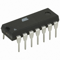
AT89LP214-20PU Atmel, AT89LP214-20PU Datasheet - Page 8

AT89LP214-20PU
Manufacturer Part Number
AT89LP214-20PU
Description
MCU 8051 2K FLASH 20MHZ 14-PDIP
Manufacturer
Atmel
Series
89LPr
Datasheet
1.AT89LP213-20PU.pdf
(98 pages)
Specifications of AT89LP214-20PU
Core Processor
8051
Core Size
8-Bit
Speed
20MHz
Connectivity
SPI, UART/USART
Peripherals
Brown-out Detect/Reset, POR, PWM, WDT
Number Of I /o
12
Program Memory Size
2KB (2K x 8)
Program Memory Type
FLASH
Ram Size
128 x 8
Voltage - Supply (vcc/vdd)
2.4 V ~ 5.5 V
Oscillator Type
Internal
Operating Temperature
-40°C ~ 85°C
Package / Case
14-DIP (0.300", 7.62mm)
Processor Series
AT89x
Core
8051
Data Bus Width
8 bit
Data Ram Size
128 B
Interface Type
SPI/UART
Maximum Clock Frequency
20 MHz
Number Of Programmable I/os
12
Number Of Timers
2
Operating Supply Voltage
2.4 V to 5 V
Maximum Operating Temperature
+ 85 C
Mounting Style
Through Hole
3rd Party Development Tools
PK51, CA51, A51, ULINK2
Development Tools By Supplier
AT89ISP
Minimum Operating Temperature
- 40 C
Lead Free Status / RoHS Status
Lead free / RoHS Compliant
Eeprom Size
-
Data Converters
-
Lead Free Status / Rohs Status
Lead free / RoHS Compliant
6.2
8
Data Memory
AT89LP213/214
A map of the AT89LP213/214 program memory is shown in
code space from 0000h to 07FFh, the AT89LP213/214 also supports a 64-byte User Signature
Array and a 32-byte Atmel Signature Array that are accessible by the CPU in a read-only fash-
ion. In order to read from the signature arrays, the SIGEN bit in AUXR1 must be set. While
SIGEN is one, MOVC A,@A+DPTR will access the signature arrays. The User Signature Array
is mapped to addresses 0040h to 007Fh and the Atmel Signature Array is mapped to addresses
0000h to 001Fh. SIGEN must be cleared before using MOVC to access the code memory.
The Atmel Signature Array is initialized with the Device ID in the factory. The User Signature
Array is available for user identification codes or constant parameter data. Data stored in the sig-
nature array is not secure. Security bits will disable writes to the array; however, reads are
always allowed.
Table 6-1.
The AT89LP213/214 contains 128 bytes of general SRAM data memory plus 128 bytes of I/O
memory mapped into a single 8-bit address space. The 128 bytes of data memory may be
accessed through both direct and indirect addressing of the lower 128 byte addresses. The 128
bytes of I/O memory reside in the upper 128 byte address space
can only be accessed through direct addressing and contains the Special Function Registers
(SFRs). Indirect accesses to the upper 128 byte addresses will return invalid data. The lowest
32 bytes of data memory are grouped into 4 banks of 8 registers each. The RS0 and RS1 bits
(PSW.3 and PSW.4) select which register bank is in use. Instructions using register addressing
will only access the currently specified bank. The AT89LP213/214 does not support external
data memory.
Figure 6-2.
LO WER
UPPER
128
128
AUXR1 = A2H
Not Bit Addressable
Bit
FFH
80H
7F H
0
–
7
AUXR1
Data Memory Map
and Indirect
Addressing
Addressing
Accessible
Accessible
– Auxiliary Register 1
By Direct
By Direct
–
6
Only
Only
–
5
–
4
Special Function
Registers
SIGEN
3
Figure
Reset Value = XXXX 0XXXB
–
2
(Figure
6-1. In addition to the 2K
Ports
Status and Control Bits
Timers
Registers
Stack Pointer
Accumulator
(Etc.)
6-2). The I/O memory
–
1
3538E–MICRO–11/10
–
0


