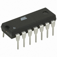
AT89LP214-20PU Atmel, AT89LP214-20PU Datasheet - Page 40

AT89LP214-20PU
Manufacturer Part Number
AT89LP214-20PU
Description
MCU 8051 2K FLASH 20MHZ 14-PDIP
Manufacturer
Atmel
Series
89LPr
Datasheet
1.AT89LP213-20PU.pdf
(98 pages)
Specifications of AT89LP214-20PU
Core Processor
8051
Core Size
8-Bit
Speed
20MHz
Connectivity
SPI, UART/USART
Peripherals
Brown-out Detect/Reset, POR, PWM, WDT
Number Of I /o
12
Program Memory Size
2KB (2K x 8)
Program Memory Type
FLASH
Ram Size
128 x 8
Voltage - Supply (vcc/vdd)
2.4 V ~ 5.5 V
Oscillator Type
Internal
Operating Temperature
-40°C ~ 85°C
Package / Case
14-DIP (0.300", 7.62mm)
Processor Series
AT89x
Core
8051
Data Bus Width
8 bit
Data Ram Size
128 B
Interface Type
SPI/UART
Maximum Clock Frequency
20 MHz
Number Of Programmable I/os
12
Number Of Timers
2
Operating Supply Voltage
2.4 V to 5 V
Maximum Operating Temperature
+ 85 C
Mounting Style
Through Hole
3rd Party Development Tools
PK51, CA51, A51, ULINK2
Development Tools By Supplier
AT89ISP
Minimum Operating Temperature
- 40 C
Lead Free Status / RoHS Status
Lead free / RoHS Compliant
Eeprom Size
-
Data Converters
-
Lead Free Status / Rohs Status
Lead free / RoHS Compliant
Table 17-1.
Notes:
40
SCON Address = 98H
Bit Addressable
Bit
Symbol
FE
SM0
SM1
SM2
REN
TB8
RB8
TI
RI
(SMOD0 = 0/1)
1. SMOD0 is located at PCON.6.
2. f
AT89LP213/214
SM0/FE
osc
Function
Framing error bit. This bit is set by the receiver when an invalid stop bit is detected. The FE bit is not cleared by valid
frames and must be cleared by software. The SMOD0 bit must be set to enable access to the FE bit. FE will be set
regardless of the state of SMOD0.
Serial Port Mode Bit 0, (SMOD0 must = 0 to access bit SM0)
Serial Port Mode Bit 1
Enables the Automatic Address Recognition feature in Modes 2 or 3. If SM2 = 1 then Rl will not be set unless the received
9th data bit (RB8) is 1, indicating an address, and the received byte is a Given or Broadcast Address. In Mode 1, if SM2 =
1 then Rl will not be activated unless a valid stop bit was received, and the received byte is a Given or Broadcast Address.
In Mode 0, SM2 should be 0.
Enables serial reception. Set by software to enable reception. Clear by software to disable reception.
The 9th data bit that will be transmitted in Modes 2 and 3. Set or clear by software as desired.
In Modes 2 and 3, the 9th data bit that was received. In Mode 1, if SM2 = 0, RB8 is the stop bit that was received. In Mode
0, RB8 is not used.
Transmit interrupt flag. Set by hardware at the end of the 8th bit time in Mode 0, or at the beginning of the stop bit in the
other modes, in any serial transmission. Must be cleared by software.
Receive interrupt flag. Set by hardware at the end of the 8th bit time in Mode 0, or halfway through the stop bit time in the
other modes, in any serial reception (except see SM2). Must be cleared by software.
7
SCON – Serial Port Control Register
= oscillator frequency.
SM0
0
0
1
1
(1)
bit and prepares to receive the data bytes that follows. The slaves that are not addressed set
their SM2 bits and ignore the data bytes.
The SM2 bit has no effect in Mode 0 but can be used to check the validity of the stop bit in
Mode 1. In a Mode 1 reception, if SM2 = 1, the receive interrupt is not activated unless a valid
stop bit is received.
SM1
6
SM1
0
1
0
1
SM2
5
Mode
0
1
2
3
REN
4
Description
shift register
8-bit UART
9-bit UART
9-bit UART
TB8
See “Automatic Address Recognition” on page
3
variable (Timer 1)
variable (Timer 1)
RB8
f
osc
Baud Rate
2
/32 or f
f
osc
/2
osc
(2)
Reset Value = 0000 0000B
/16
T1
1
3538E–MICRO–11/10
RI
0
49.


